ꢀ ꢁꢂ ꢃ ꢄ ꢄ ꢅ ꢆꢇ ꢈꢈ ꢂ ꢄ ꢄ ꢅ ꢆ ꢇꢉ ꢈꢂ ꢄꢄ
ꢊ ꢋꢌꢍꢎ ꢋꢏꢐ ꢑ ꢐ ꢒꢇꢑ ꢍ ꢎꢒ ꢓ ꢑꢎ ꢆ
SLLS094C − SEPTEMBER 1983 − REVISED MAY 2004
†
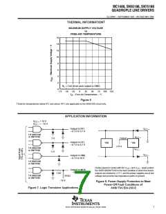
THERMAL INFORMATION
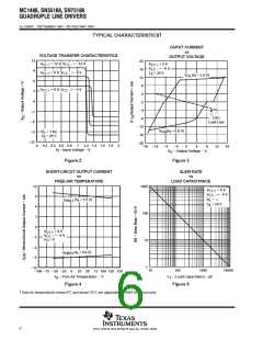
MAXIMUM SUPPLY VOLTAGE
vs
FREE-AIR TEMPERATURE
16
14
12
10
8
6
4
2
R
≥ 3 kΩ (from each output to GND)
L
0
−75 −50 −25
0
25
50
75 100 125
T
A
− Free-Air Temperature − °C
Figure 6
†
Data for temperatures below 0°C and above 70°C are applicable to the SN55188 circuit only.
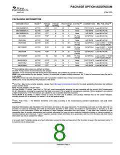
APPLICATION INFORMATION
V
CC+
V
CC−
= 12 V
= −12 V
Output to RTL
−0.7 V to 3.7 V
V
CC+
1/4 SN55188
or SN75188
V
CC+
3 V
5 V
Output
Output to DTL
−0.7 V to 5.7 V
’188
’188
15 V
1/4 SN55188
or SN75188
V
CC−
V
CC−
Output to HNIL
−0.7 V to 10 V
1/4 SN55188
or SN75188
Diodes placed in series with the V
CC+
and V leads protect
CC−
Output to MOS
−10 V to 0 V
the SN55188/SN75188 in the fault condition in which the device
outputs are shorted to 15 V, and the power supplies are at low
voltage and provide low-impedance paths to ground.
1 kΩ
1/4 SN55188
or SN75188
10 kΩ
−12 V
Figure 8. Power-Supply Protection to Meet
Power-Off Fault Conditions of
ANSI TIA/EIA-232-E
Figure 7. Logic Translator Applications
7
POST OFFICE BOX 655303 • DALLAS, TEXAS 75265

 TI [ TEXAS INSTRUMENTS ]