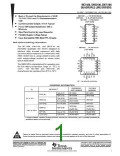
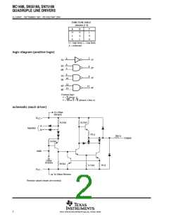
ꢀ ꢁꢂ ꢃ ꢄ ꢄ ꢅ ꢆꢇ ꢈꢈ ꢂ ꢄ ꢄ ꢅ ꢆ ꢇꢉ ꢈꢂ ꢄꢄ
ꢊ ꢋꢌꢍꢎ ꢋꢏꢐ ꢑ ꢐ ꢒꢇꢑ ꢍ ꢎꢒ ꢓ ꢑꢎ ꢆ
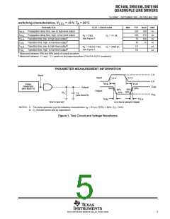
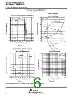
SLLS094C − SEPTEMBER 1983 − REVISED MAY 2004
†
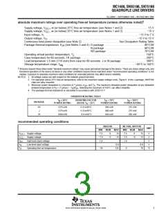
absolute maximum ratings over operating free-air temperature (unless otherwise noted)
Supply voltage, V
Supply voltage, V
at (or below) 25°C free-air temperature (see Notes 1 and 2) . . . . . . . . . . . . . . . . . 15 V
at (or below) 25°C free-air temperature (see Notes 1 and 2) . . . . . . . . . . . . . . . . −15 V
CC+
CC−
Input voltage, V . . . . . . . . . . . . . . . . . . . . . . . . . . . . . . . . . . . . . . . . . . . . . . . . . . . . . . . . . . . . . . . . . . . . −15 V to 7 V
I
Output voltage, V . . . . . . . . . . . . . . . . . . . . . . . . . . . . . . . . . . . . . . . . . . . . . . . . . . . . . . . . . . . . . . . . . −15 V to 15 V
O
Continuous total power dissipation (see Note 2) . . . . . . . . . . . . . . . . . . . . . . . . . . See Dissipation Rating Table
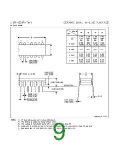
Package thermal impedance, θ (see Notes 3 and 4): D package . . . . . . . . . . . . . . . . . . . . . . . . . . . . 86°C/W
JA
N package . . . . . . . . . . . . . . . . . . . . . . . . . . . . 80°C/W
NS package . . . . . . . . . . . . . . . . . . . . . . . . . . . 76°C/W
Operating virtual junction temperature, T . . . . . . . . . . . . . . . . . . . . . . . . . . . . . . . . . . . . . . . . . . . . . . . . . . . 150°C
J
Case temperature for 60 seconds, FK package . . . . . . . . . . . . . . . . . . . . . . . . . . . . . . . . . . . . . . . . . . . . . . 260°C
Lead temperature 1,6 mm (1/16 inch) from case for 60 seconds: J or W package . . . . . . . . . . . . . . . . 300°C
Storage temperature range, T
. . . . . . . . . . . . . . . . . . . . . . . . . . . . . . . . . . . . . . . . . . . . . . . . . . . −65°C to 150°C
stg
†
Stresses beyond those listed under “absolute maximum ratings” may cause permanent damage to the device. These are stress ratings only, and
functional operation of the device at these or any other conditions beyond those indicated under “recommended operating conditions” is not
implied. Exposure to absolute-maximum-rated conditions for extended periods may affect device reliability.
NOTES: 1. All voltage values are with respect to the network ground terminal.
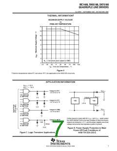
2. For operation above 25°C free-air temperature, refer to the maximum supply voltage curve, Figure 6. In the J package, SN55188
chips are alloy mounted.
3. Maximum power dissipation is a function of T (max), θ , and T . The maximum allowable power dissipation at any allowable
JA
J
A
ambient temperature is P = (T (max) − T )/θ . Selecting the maximum of 150°C can affect reliability.
D
J
A
JA
4. The package thermal impedance is calculated in accordance with JESD 51-7.
DISSIPATION RATING TABLE
T
≤ 25°C
DERATING FACTOR
T
= 70°C
T = 125°C
A
POWER RATING
A
A
PACKAGE
POWER RATING
ABOVE T = 25°C
POWER RATING
A
FK
J
1375 mW
1375 mW
1000 mW
11.0 mW/°C
11.0 mW/°C
8.0 mW/°C
880 mW
880 mW
640 mW
275 mW
275 mW
200 mW
W
recommended operating conditions
SN55188
MC1488, SN75188
UNIT
MIN NOM
MAX
15
MIN NOM
MAX
V
V
V
V
Supply voltage
7.5
−7.5
1.9
9
7.5
−7.5
1.9
9
15
V
V
CC+
CC−
IH
Supply voltage
−9
−15
−9
−15
High-level input voltage
Low-level input voltage
Operating free-air temperature
V
0.8
0.8
70
V
IL
T
A
−55
125
0
°C
3
POST OFFICE BOX 655303 • DALLAS, TEXAS 75265

 TI [ TEXAS INSTRUMENTS ]