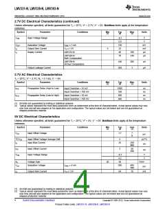
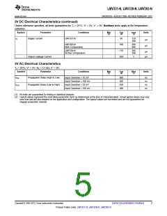
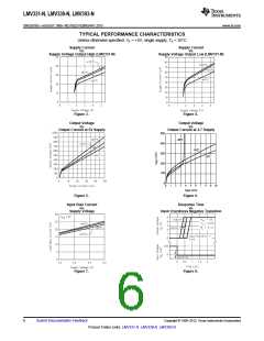
LMV331-N, LMV339-N, LMV393-N
SNOS018G –AUGUST 1999–REVISED FEBRUARY 2013
www.ti.com
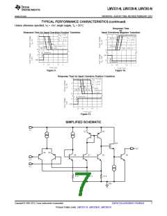
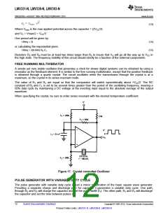
APPLICATION CIRCUITS
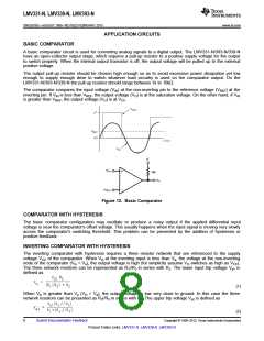
BASIC COMPARATOR
A basic comparator circuit is used for converting analog signals to a digital output. The LMV331-N/393-N/339-N
have an open-collector output stage, which requires a pull-up resistor to a positive supply voltage for the output
to switch properly. When the internal output transistor is off, the output voltage will be pulled up to the external
positive voltage.
The output pull-up resistor should be chosen high enough so as to avoid excessive power dissipation yet low
enough to supply enough drive to switch whatever load circuitry is used on the comparator output. On the
LMV331-N/393-N/339-N the pull-up resistor should range between 1k to 10kΩ.
The comparator compares the input voltage (VIN) at the non-inverting pin to the reference voltage (VREF) at the
inverting pin. If VIN is less than VREF, the output voltage (VO) is at the saturation voltage. On the other hand, if VIN
is greater than VREF, the output voltage (VO) is at VCC
.
Figure 12. Basic Comparator
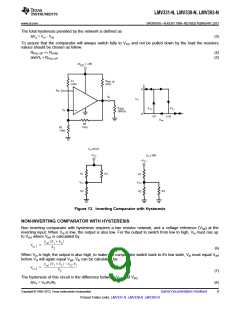
COMPARATOR WITH HYSTERESIS
The basic comparator configuration may oscillate or produce a noisy output if the applied differential input
voltage is near the comparator's offset voltage. This usually happens when the input signal is moving very slowly
across the comparator's switching threshold. This problem can be prevented by the addition of hysteresis or
positive feedback.
INVERTING COMPARATOR WITH HYSTERESIS
The inverting comparator with hysteresis requires a three resistor network that are referenced to the supply
voltage VCC of the comparator. When Vin at the inverting input is less than Va, the voltage at the non-inverting
node of the comparator (Vin < Va), the output voltage is high (for simplicity assume VO switches as high as VCC).
The three network resistors can be represented as R1//R3 in series with R2. The lower input trip voltage Va1 is
defined as
(1)
When Vin is greater than Va (Vin > Va), the output voltage is low very close to ground. In this case the three
network resistors can be presented as R2//R3 in series with R1. The upper trip voltage Va2 is defined as
(2)
8
Submit Documentation Feedback
Copyright © 1999–2013, Texas Instruments Incorporated
Product Folder Links: LMV331-N LMV339-N LMV393-N

 TI [ TEXAS INSTRUMENTS ]