Symbol
Parameter
Conditions
Min
4.7
Typ
Max
Units
Bus free time between a STOP and START
condition
tBUF
µs
tVD;DAT
tVD;ACK
tSP
Data valid time
3.45
3.45
µs
µs
Data valid acknowledge time
Pulse width of spikes that must be
suppressed by the input filter(Note 14)
50
ns
t_timeout SCL and SDA Timeout
25
100
ms
ns
ns
tEN;START
tEN;STOP
tEN;HIGH
I2C Interface Enabling
I2C Interface Disabling
600
600
time between consecutive I2C interface
enabling and disabling
600
ns
Note 1: “Absolute Maximum Ratings” indicate limits beyond which damage to the device may occur, including inoperability and degradation of device reliability
and/or performance. Functional operation of the device and/or non-degradation at the Absolute Maximum Ratings or other conditions beyond those indicated in
the Operating Ratings is not implied. Operating Ratings indicate conditions at which the device is functional and the device should not be operated beyond such
conditions.
Note 2: Human Body Model, applicable std. MIL-STD-883, Method 3015.7. Machine Model, applicable std. JESD22-A115-A (ESD MM std. of JEDEC) Field-
Induced Charge-Device Model, applicable std. JESD22-C101-C (ESD FICDM std. of JEDEC).
Note 3: All non-power pins of this device are protected against ESD by snapback devices. Voltage at such pins will rise beyond absmax if current is forced into
pin.
Note 4: The maximum power dissipation is a function of TJ(MAX), θJA, and the ambient temperature, TA. The maximum allowable power dissipation at any ambient
temperature is PDMAX = (TJ(MAX) - TA)/ θJA All numbers apply for packages soldered directly onto a PC board.
Note 5: Electrical Table values apply only for factory testing conditions at the temperature indicated. Factory testing conditions result in very limited self-heating
of the device such that TJ = TA. No guarantee of parametric performance is indicated in the electrical tables under conditions of internal self-heating where TJ >
TA. Absolute Maximum Ratings indicate junction temperature limits beyond which the device may be permanently degraded, either mechanically or electrically.
Note 6: Typical values represent the most likely parametric norm as determined at the time of characterization. Actual typical values may vary over time and will
also depend on the application and configuration. The typical values are not tested and are not guaranteed on shipped production material.
Note 7: Limits are 100% production tested at 25°C. Limits over the operating temperature range are guaranteed through correlations using statistical quality
control (SQC) method.
Note 8: Offset voltage temperature drift is determined by dividing the change in VOS at the temperature extremes by the total temperature change.
Starting from the measured voltage offset at temperature T1 (VOS_RW(T1)), the voltage offset at temperature T2 (VOS_RW(T2)) is calculated according the following
formula: VOS_RW(T2)=VOS_RW(T1)+ABS(T2–T1)* TcVOS_RW
.
Note 9: At such currents no accuracy of the output voltage can be expected.
Note 10: This parameter includes both A1 and TIA's noise contribution.
Note 11: In case of external reference connected, the noise of the reference has to be added.
Note 12: For negative bias polarity the Internal Zero is set at 67% VREF.
Note 13: LMP91000 provides an internal 300ns minimum hold time to bridge the undefined region of the falling edge of SCL.
Note 14: This parameter is guaranteed by design or characterization.
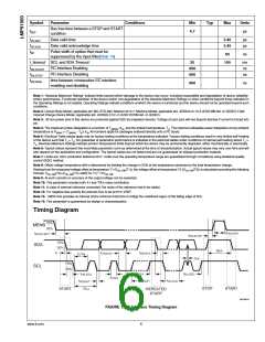
Timing Diagram
30132541
FIGURE 1. I2C Interface Timing Diagram
www.ti.com
6

 TI [ TEXAS INSTRUMENTS ]