For soldering specifications:
see product folder at www.national.com and
www.national.com/ms/MS/MS-SOLDERING.pdf
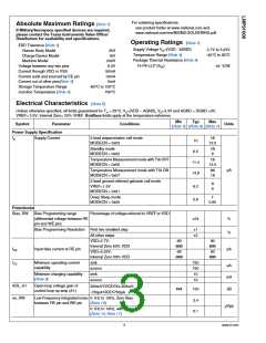
Absolute Maximum Ratings (Note 1)
If Military/Aerospace specified devices are required,
please contact the Texas Instruments Sales Office/
Distributors for availability and specifications.
Operating Ratings (Note 1)
Supply Voltage VS=(VDD - AGND)
ESD Tolerance (Note 2)
Human Body Model
2.7V to 5.25V
-40°C to 85°C
2kV
Temperature Range (Note 4)
Package Thermal Resistance (Note 4)
Charge-Device Model
Machine Model
1kV
200V
14-Pin LLP (θJA
)
44 °C/W
Voltage between any two pins
Current through VDD or VSS
Current sunk and sourced by CE pin
Current out of other pins(Note 3)
Storage Temperature Range
Junction Temperature (Note 4)
6.0V
50mA
10mA
5mA
-65°C to 150°C
150°C
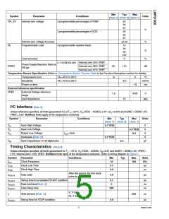
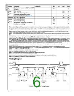
Electrical Characteristics (Note 5)
Unless otherwise specified, all limits guaranteed for TA = 25°C, VS=(VDD – AGND), VS=3.3V and AGND = DGND =0V,
VREF= 2.5V, Internal Zero= 20% VREF. Boldface limits apply at the temperature extremes.
Min
Typ
Max
Symbol
Parameter
Conditions
Units
(Note 7) (Note 6) (Note 7)
Power Supply Specification
IS
Supply Current
3-lead amperometric cell mode
MODECN = 0x03
15
13.5
10
Standby mode
MODECN = 0x02
10
6.5
8
Temperature Measurement mode with TIA OFF
MODECN = 0x06
15
11.4
13.5
µA
Temperature Measurement mode with TIA ON
MODECN = 0x07
20
14.9
18
2-lead ground referred galvanic cell mode
VREF=1.5V
MODECN = 0x01
9
6.2
8
Deep Sleep mode
MODECN = 0x00
1
0.6
0.85
Potentiostat
Bias_RW
Bias Programming range
(differential voltage between RE
pin and WE pin)
Percentage of voltage referred to VREF or VDD
±24
%
%
Bias Programming Resolution First two smallest step
±1
±2
All other steps
VDD=2.7V;
-90
90
Internal Zero 50% VDD
Input bias current at RE pin
-800
800
IRE
pA
VDD=5.25V;
-90
90
Internal Zero 50% VDD
-900
900
ICE
Minimum operating current
capability
sink
750
750
10
µA
mA
dB
source
sink
Minimum charging capability
(Note 9)
source
10
AOL_A1
en_RW
Open loop voltage gain of
control loop op amp (A1)
300mV≤VCE≤Vs-300mV;
-750µA≤ICE≤750µA
104
120
Low Frequency integrated noise 0.1Hz to 10Hz, Zero Bias
between RE pin and WE pin
3.4
5.1
(Note 10)
µVpp
0.1Hz to 10Hz, with Bias
(Note 10, Note 11)
3
www.ti.com

 TI [ TEXAS INSTRUMENTS ]