Min
Typ
Max
Symbol
Parameter
Conditions
Units
(Note 7) (Note 6) (Note 7)
TIA_ZV
Internal zero voltage
3 programmable percentages of VREF
20
50
67
%
3 programmable percentages of VDD
4 programmable resistive loads
20
50
67
Internal zero voltage Accuracy
Programmable Load
±0.04
%
RL
10
33
50
Ω
100
Load accuracy
5
%
Internal zero 20% VREF
2.7 ≤VDD≤5.25V
Power Supply Rejection Ratio at
RE pin
PSRR
Internal zero 50% VREF
Internal zero 67% VREF
80
110
dB
Temperature Sensor Specification (Refer to Temperature Sensor Transfer Table in the Function Description section for details)
Temperature Error
Sensitivity
TA=-40˚C to 85˚C
TA=-40˚C to 85˚C
-3
3
°C
mV/°C
ms
-8.2
10
Power on time
1.9
External reference specification
VREF
External Voltage reference
range
1.5
VDD
V
Input impedance
MΩ
I2C Interface (Note 5)
Unless otherwise specified, all limits guaranteed for at TA = 25°C, VS=(VDD – AGND), 2.7V <VS< 5.25V and AGND = DGND =0V,
VREF= 2.5V. Boldface limits apply at the temperature extremes
Symbol
Parameter
Conditions
Min
Typ
Max
Units
(Note 7) (Note 6) (Note 7)
VIH
Input High Voltage
0.7*VDD
0.3*VDD
0.4
V
V
VIL
Input Low Voltage
VOL
Output Low Voltage
IOUT=3mA
V
Hysteresis (Note 14)
0.1*VDD
0.5
V
CIN
Input Capacitance on all digital pins
pF
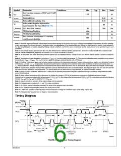
Timing Characteristics (Note 5)
Unless otherwise specified, all limits guaranteed for TA = 25°C, VS=(VDD – AGND), VS=3.3V and AGND = DGND =0V, VREF=
2.5V, Internal Zero= 20% VREF. Boldface limits apply at the temperature extremes. Refer to timing diagram in Figure 1.
Symbol
fSCL
Parameter
Conditions
Min
10
Typ
Max
100
Units
kHz
µs
Clock Frequency
Clock Low Time
Clock High Time
tLOW
4.7
4.0
tHIGH
µs
After this period, the first clock
pulse is generated
tHD;STA
Data valid
4.0
µs
tSU;STA
tHD;DAT
tSU;DAT
Set-up time for a repeated START condition
Data hold time(Note 13)
4.7
0
µs
ns
ns
Data Setup time
250
IL ≤ 3mA;
CL ≤ 400pF
tf
SDA fall time (Note 14)
250
ns
µs
tSU;STO
Set-up time for STOP condition
4.0
5
www.ti.com

 TI [ TEXAS INSTRUMENTS ]