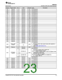
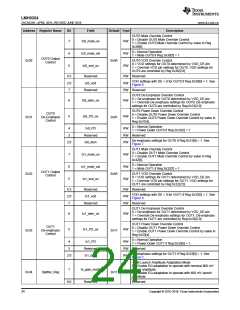
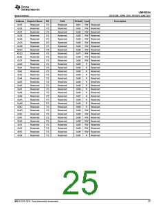
LMH0324
www.ti.com.cn
ZHCSIC8B –APRIL 2016–REVISED JUNE 2018
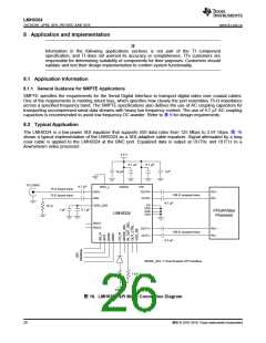
Typical Application (接下页)
8.2.1 Design Requirements
表 8. LMH0324 Design Requirements
DESIGN PARAMETER
REQUIREMENTS
AC coupling capacitor at IN0+ should be a 4.7-μF surface mount ceramic capacitor. IN0-
should be AC terminated with 4.7 μF and 75 Ω to VSS.
Input AC coupling capacitors
IN0+ and IN0- should be routed with uncoupled board traces with 75-Ω characteristic
impedance.
High speed board trace for IN0
BNC connector
High performance BNC capable to support 2.97 Gbps should be used. Footprint of the BNC
should be designed to achieve 75-Ω characteristic impedance. For achieving best return loss
performance, the BNC should be placed as close to the LMH0324 device as possible
Both OUT0± and OUT1± require AC coupling capacitors. 4.7-μF capacitors are
recommended.
Output AC coupling capacitors
High speed board trace for OUT0± and
OUT1±
OUT0± and OUT1± should be routed with coupled board traces with 100-Ω differential
impedance.
Set MODE_SEL to Level-F (pin unconnected) for SPI. Set MODE_SEL to Level-L (connect 1
kΩ to VSS) for SMBus. SMBus is 3.3 V tolerant if VDDIO is powered from 2.5 V.
Use of SPI or SMBus interface
8.2.2 Detailed Design Procedure
The following general design procedure is recommended:
1. Select a suitable power supply voltage for the LMH0324. It can be powered from a single 2.5 V or 1.8 V
supply. See Power Supply Recommendations for details.
2. Check that the power supply meets the DC and AC requirements in the Recommended Operating
Conditions.
3. Select the proper pull-high or pull-low resistors for IN_OUT_SEL and OUT_CTRL for setting the signal path.
4. If -6 dB launch amplitude or other expanded programmable features are needed, select the use of SPI or
SMBus by setting the proper pull-high or pull-low resistor for the MODE_SEL pin.
5. Choose a high quality 75-Ω BNC that is capable to support 2.97 Gbps applications. Consult a BNC supplier
regarding insertion loss, impedance specifications, and recommended BNC footprint for meeting SMPTE
return loss requirements.
6. Depending on the length and insertion loss of the output traces for OUT0± and OUT1±, select the proper
pull-high or pull-low resistors for VOD_DE to set the output amplitude and de-emphasis settings. Refer to
Table 4 for details.
7. Choose a small 0402 surface mount ceramic capacitors for the AC coupling and bypass capacitors.
8. Use proper footprint for BNC and AC coupling capacitors. Anti-pads are commonly used in power and VSS
planes under these landing pads to achieve optimum return loss.
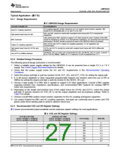
8.2.3 Recommended VOD and DE Register Settings
表 9 shows recommended output amplitude and de-emphasis register settings for most applications.
表 9. VOD and DE Register Settings
VOD REG SETTING
DEM REG SETTING
OUT0±: 0x30[5]=1, 0x30[2:0]
OUT1±: 0x32[5]=1, 0x32[2:0]
OUT0±: 0x31[6]=1, 0x31[2:0]
OUT1±: 0x33[6]=1, 0x33[2:0]
VOD (mVpp)
DEM (dB)
0
1
2
2
3
3
3
4
0
1
1
2
1
2
3
1
410
486
560
560
635
635
635
716
0
-0.1
-0.1
-0.9
-0.3
-1.3
-2.4
-0.5
版权 © 2016–2018, Texas Instruments Incorporated
27

 TI [ TEXAS INSTRUMENTS ]