LMH0324
ZHCSIC8B –APRIL 2016–REVISED JUNE 2018
www.ti.com.cn
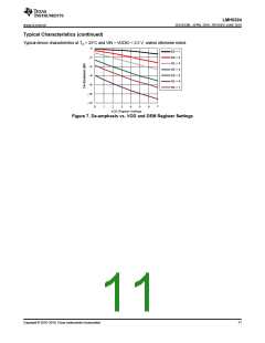
7.3.4 Launch Amplitude
The LMH0324 is designed to equalize data transmitted through a coaxial cable driven by a SMPTE compatible
cable driver with launch amplitude of 800 mVp-p ± 10%. In applications where a 1:2 passive splitter is used, the
signal amplitude is reduced by half due to the 6 dB insertion loss of the splitter. The LMH0324 is designed to
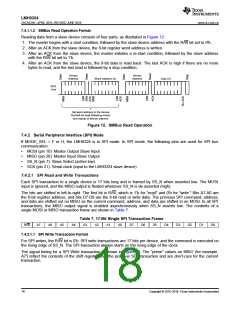
support -6 dB splitter mode, enabled by SPI or SMBus serial interface.
7.3.5 Input-Output Mux Selection
By default, the LMH0324 input-to-output signal flow and data rate selection are configured by the IN_OUT_SEL
pin logic settings shown in Table 2. These settings can be overridden via register control by applying the
appropriate override bit values.
Table 2. IN_OUT_SEL Pin Settings
LEVEL
DEFINITION
H
F
R
L
IN0 to OUT0 and OUT1
IN0 to OUT0 (with OUT1 disabled)
Reserved
Reserved
7.3.6 Output Function Control
By default, the LMH0324 output function control for OUT0 and OUT1 is configured by the OUT_CTRL pin logic
settings shown in Table 3. These settings can be overridden via register control by applying the appropriate
override bit values.
Table 3. OUT_CTRL Pin Settings
LEVEL
DEFINITION
Equalizer Bypass
Raw data at IN0+ is routed to the output drivers
H
Normal Data
Equalized data is routed to the output drivers
F
R
L
Reserved
Reserved
7.3.7 Output Driver Amplitude and De-Emphasis Control
The VOD_DE control pin selects the output amplitude and de-emphasis settings for both OUT0± and OUT1±. It
offers users the capability to select higher output amplitude and de-emphasis level for longer board trace that
connects the drivers to their downstream receivers. Driver de-emphasis provides transmitter equalization to
reduce the ISI caused by the board trace.
By default, the output driver VOD and de-emphasis settings are configured by the VOD_DE pin logic settings
shown in Table 4. These settings can be overridden via register control. Through register programming, the
output amplitude and de-emphasis level can be individually set for OUT0± and OUT1±. SPI and SMBus register
programming provide a wider range of output amplitude and de-emphasis levels.
Table 4. Recommended VOD_DE Pin and Register Settings for Different FR4 Trace Lengths(1)
VOD REG SETTING
OUT0±: 0x30[5]=1, 0x30[2:0]
OUT1±: 0x32[5]=1, 0x32[2:0]
DEM REG SETTING
OUT0±: 0x31[6]=1, 0x31[2:0]
OUT1±: 0x33[6]=1, 0x33[2:0]
FR4 TRACE
LENGTH
(inches)
VOD_DE
LEVEL
VOD
VODDE
DEM (dB)
(mVpp)(2)
(mVpp)(2)
H
F
R
L
0
2
3
5
0
2
3
5
410
560
635
810
410
500
480
480
0
0 – 1
2 – 4
5 – 6
7 – 8
-0.9
-2.4
-6.1
(1) The output drivers are capable of providing higher VOD and DEM levels (max settings are 7). For more VOD and de-emphasis levels,
refer to 表 9.
(2) See Figure 8.
14
Copyright © 2016–2018, Texas Instruments Incorporated

 TI [ TEXAS INSTRUMENTS ]