LM555
SNAS548C –FEBRUARY 2000–REVISED MARCH 2013
www.ti.com
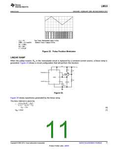
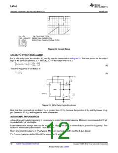
VCC = 5V
Top Trace: Input 3V/Div.
TIME = 20μs/DIV. Middle Trace: Output 5V/Div.
R1 = 47kΩ
Bottom Trace: Capacitor Voltage 1V/Div.
R2 = 100kΩ
RE = 2.7 kΩ
C = 0.01 μF
Figure 24. Linear Ramp
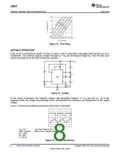
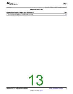
50% DUTY CYCLE OSCILLATOR
For a 50% duty cycle, the resistors RA and RB may be connected as in Figure 25. The time period for the output
high is the same as previous, t1 = 0.693 RA C. For the output low it is t2 =
(8)
Thus the frequency of oscillation is:
(9)
Figure 25. 50% Duty Cycle Oscillator
Note that this circuit will not oscillate if RB is greater than 1/2 RA because the junction of RA and RB cannot bring
pin 2 down to 1/3 VCC and trigger the lower comparator.
ADDITIONAL INFORMATION
Adequate power supply bypassing is necessary to protect associated circuitry. Minimum recommended is 0.1μF
in parallel with 1μF electrolytic.
Lower comparator storage time can be as long as 10μs when pin 2 is driven fully to ground for triggering. This
limits the monostable pulse width to 10μs minimum.
Delay time reset to output is 0.47μs typical. Minimum reset pulse width must be 0.3μs, typical.
Pin 7 current switches within 30ns of the output (pin 3) voltage.
12
Submit Documentation Feedback
Copyright © 2000–2013, Texas Instruments Incorporated
Product Folder Links: LM555

 TI [ TEXAS INSTRUMENTS ]