LM5116
SNVS499G –FEBRUARY 2007–REVISED MARCH 2013
www.ti.com
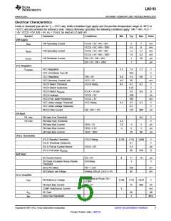
Absolute Maximum Ratings(1)(2)
VIN to GND
VCC, VCCX, UVLO to GND(3)
SW, CS to GND
HB to SW
-0.3V to 100V
-0.3 to 16V
-3.0 to 100V
-0.3 to 16V
-0.3 to HB+0.3V
-0.3 to 100V
-1V to 1V
HO to SW
VOUT to GND
CSG to GND
LO to GND
-0.3 to VCC+0.3V
-0.3 to 7V
SS to GND
FB to GND
-0.3 to 7V
DEMB to GND
-0.3 to VCC
-0.3 to 7V
RT to GND
EN to GND
-0.3 to 100V
2 kV
ESD Rating HBM(4)
Storage Temperature Range
Junction Temperature
-55°C to +150°C
+150°C
(1) Absolute Maximum Ratings indicate limits beyond which damage to the component may occur.
(2) If Military/Aerospace specified devices are required, please contact the Texas Instruments Sales Office/Distributors for availability and
specifications.
(3) These pins must not exceed VIN.
(4) The human body model is a 100 pF capacitor discharged through a 1.5 kΩ resistor into each pin. 2 kV rating for all pins except VIN
which is rated for 1.5 kV.
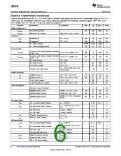
Operating Ratings(1)(2)
VIN
6V to 100V
4.75V to 15V
4.75V to 15V
-0.3V to 2V
VCC, VCCX
HB to SW
DEMB to GND
Junction Temperature
-40°C to +125°C
(1) RAMP, COMP are output pins. As such they are not specified to have an external voltage applied.
(2) Operating Ratings do not imply performance limits. For specified performance limits and associated test conditions, see the Electrical
Characteristics tables.
4
Submit Documentation Feedback
Copyright © 2007–2013, Texas Instruments Incorporated
Product Folder Links: LM5116

 TI [ TEXAS INSTRUMENTS ]