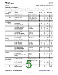
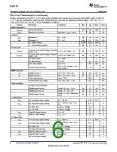
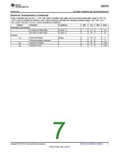
LM5116
www.ti.com
SNVS499G –FEBRUARY 2007–REVISED MARCH 2013
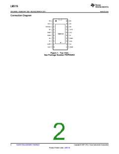
PIN DESCRIPTIONS
Pin
1
Name
Description
VIN
Chip supply voltage, input voltage monitor and input to the VCC regulator.
2
UVLO
If the UVLO pin is below 1.215V, the regulator will be in standby mode (VCC regulator running, switching regulator
disabled). If the UVLO pin voltage is above 1.215V, the regulator is operational. An external voltage divider can be used
to set an under-voltage shutdown threshold. There is a fixed 5 µA pull up current on this pin when EN is high. UVLO is
pulled to ground in the event a current limit condition exists for 256 clock cycles.
3
RT/SYN The internal oscillator is set with a single resistor between this pin and the AGND pin. The recommended frequency
C
range is 50 kHz to 1 MHz. The internal oscillator can be synchronized to an external clock by AC coupling a positive
edge onto this node.
4
5
EN
If the EN pin is below 0.5V, the regulator will be in a low power state drawing less than 10 µA from VIN. EN must be
pulled above 3.3V for normal operation. The maximum EN transition time for proper operation is one switching period.
RAMP Ramp control signal. An external capacitor connected between this pin and the AGND pin sets the ramp slope used for
current mode control.
6
7
AGND Analog ground.Connect to PGND through the exposed pad ground connection under the LM5116.
SS
An external capacitor and an internal 10 µA current source set the soft start time constant for the rise of the error amp
reference. The SS pin is held low during VCC < 4.5V, UVLO < 1.215V, EN input low or thermal shutdown.
8
9
FB
Feedback signal from the regulated output. This pin is connected to the inverting input of the internal error amplifier. The
regulation threshold is 1.215V.
COMP Output of the internal error amplifier. The loop compensation network should be connected between this pin and the FB
pin.
10
11
VOUT
Output monitor. Connect directly to the output voltage.
DEMB Low-side MOSFET source voltage monitor for diode emulation. For start-up into a pre-biased load, tie this pin to ground
at the CSG connection. For fully synchronous operation, use an external series resistor between DEMB and ground to
raise the diode emulation threshold above the low-side SW on-voltage.
12
13
CS
Current sense amplifier input. Connect to the top of the current sense resistor or the drain of the low-sided MOSFET if
RDS(ON) current sensing is used.
CSG
Current sense amplifier input. Connect to the bottom of the sense resistor or the source of the low-side MOSFET if
RDS(ON) current sensing is used.
14
15
16
17
PGND Power ground. Connect to AGND through the exposed pad ground connection under the LM5116.
LO
Connect to the gate of the low-side synchronous MOSFET through a short, low inductance path.
Locally decouple to PGND using a low ESR/ESL capacitor located as close to the controller as possible.
VCC
VCCX
Optional input for an externally supplied VCC. If VCCX > 4.5V, VCCX is internally connected to VCC and the internal
VCC regulator is disabled. If VCCX is unused, it should be connected to ground.
18
HB
High-side driver supply for bootstrap gate drive. Connect to the cathode of the bootstrap diode and the positive terminal
of the bootstrap capacitor. The bootstrap capacitor supplies current to charge the high-side MOSFET gate and should be
placed as close to the controller as possible.
19
20
HO
SW
Connect to the gate of the high-side synchronous MOSFET through a short, low inductance path
Switch node. Connect to the negative terminal of the bootstrap capacitor and the source terminal of the high-side
MOSFET.
EP
EP
Exposed pad. Solder to ground plane.
These devices have limited built-in ESD protection. The leads should be shorted together or the device placed in conductive foam
during storage or handling to prevent electrostatic damage to the MOS gates.
Copyright © 2007–2013, Texas Instruments Incorporated
Submit Documentation Feedback
3
Product Folder Links: LM5116

 TI [ TEXAS INSTRUMENTS ]