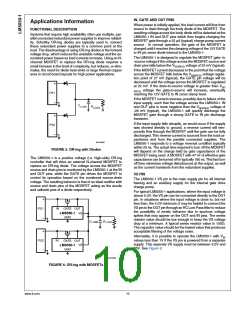
Selecting a MOSFET with an RDS(ON) that is too large will re-
sult in excessive power dissipation. Additionally, the MOS-
FET gate will be charged to the full value that the LM5050-1
can provide as it attempts to drive the Drain to Source voltage
down to the VSD(REG) of 22 mV typical. This increased Gate
charge will require some finite amount of additional discharge
time when the MOSFET needs to be turned off.
reasonably well controlled, since the RDS(ON) of the MOSFET
increases as the junction temperature increases.
PDISS = ID2 x (RDS(ON)
)
Operating with a maximum ambient temperature (TA(MAX)) of
35°C, a load current of 10A, and an RDS(ON) of 10 mΩ, and
desiring to keep the junction temperature under 100°C, the
maximum junction-to-ambient thermal resistance rating (θJA
would need to be:
)
As a guideline, it is suggest that RDS(ON) be selected to provide
at least 22 mV, and no more than 100 mV, at the nominal load
current.
θJA ≤ (TJ(MAX) - TA(MAX))/(ID2 x RDS(ON)
)
(22 mV / ID) ≤ RDS(ON) ≤ (100mV / ID)
The thermal resistance of the MOSFET package should also
be considered against the anticipated dissipation in the MOS-
FET in order to ensure that the junction temperature (TJ) is
θJA ≤ (100°C - 35°C)/(10A x 10A x 0.01Ω)
θJA ≤ 65°C/W
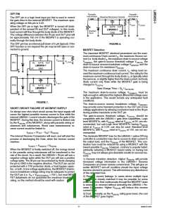
Typical Applications
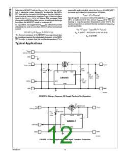
30104845
FIGURE 9. Using a Separate VS Supply For Low Vin Operation
30104842
FIGURE 10. Basic Application with Input Transient Protection
www.ti.com
12

 TI [ TEXAS INSTRUMENTS ]