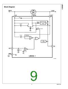
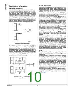
IN, GATE AND OUT PINS
Applications Information
When power is initially applied, the load current will flow from
source to drain through the body diode of the MOSFET. The
resulting voltage across the body diode will be detected at the
LM5050-1 IN and OUT pins which then begins charging the
MOSFET gate through a 32 µA (typical) charge pump current
source . In normal operation, the gate of the MOSFET is
charged until it reaches the clamping voltage of the 12V GATE
to IN pin zener diode internal to the LM5050-1.
FUNCTIONAL DESCRIPTION
Systems that require high availability often use multiple, par-
allel-connected redundant power supplies to improve reliabil-
ity. Schottky OR-ing diodes are typically used to connect
these redundant power supplies to a common point at the
load. The disadvantage of using OR-ing diodes is the forward
voltage drop, which reduces the available voltage and the as-
sociated power losses as load currents increase. Using an N-
channel MOSFET to replace the OR-ing diode requires a
small increase in the level of complexity, but reduces, or elim-
inates, the need for diode heat sinks or large thermal copper
area in circuit board layouts for high power applications.
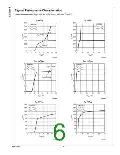
The LM5050-1 is designed to regulate the MOSFET gate- to
-source voltage if the voltage across the MOSFET source and
drain pins falls below the VSD(REG) voltage of 22 mV (typical).
If the MOSFET current decreases to the point that the voltage
across the MOSFET falls below the VSD(REG) voltage regula-
tion point of 27 mV (typical), the GATE pin voltage will be
decreased until the voltage across the MOSFET is regulated
at 22 mV. If the drain-to-source voltage is greater than VSD
voltage the gate-to-source will increase, eventually
(REG)
reaching the 12V GATE to IN zener clamp level.
If the MOSFET current reverses, possibly due to failure of the
input supply, such that the voltage across the LM5050-1 IN
and OUT pins is more negative than the VSD(REV) voltage of
-28 mV (typical), the LM5050-1 will quickly discharge the
MOSFET gate through a strong GATE to IN pin discharge
transistor.
If the input supply fails abruptly, as would occur if the supply
was shorted directly to ground, a reverse current will tem-
porarily flow through the MOSFET until the gate can be fully
discharged. This reverse current is sourced from the load ca-
pacitance and from the parallel connected supplies. The
LM5050-1 responds to a voltage reversal condition typically
within 25 ns. The actual time required to turn off the MOSFET
will depend on the charge held by gate capacitance of the
MOSFET being used. A MOSFET with 47 nF of effective gate
capacitance can be turned off in typically 180 ns. This fast turn
off time minimizes voltage disturbances at the output, as well
as the current transients from the redundant supplies.
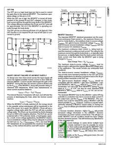
30104832
FIGURE 5. OR-ing with Diodes
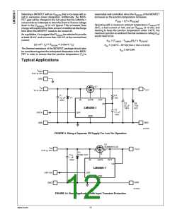
The LM5050-1 is a positive voltage (i.e. high-side) OR-ing
controller that will drive an external N-channel MOSFET to
replace an OR-ing diode. The voltage across the MOSFET
source and drain pins is monitored by the LM5050-1 at the IN
and OUT pins, while the GATE pin drives the MOSFET to
control its operation based on the monitored source-drain
voltage. The resulting behavior is that of an ideal rectifier with
source and drain pins of the MOSFET acting as the anode
and cathode pins of a diode respectively.
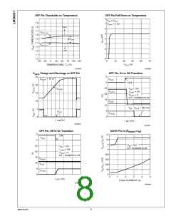
VS PIN
The LM5050-1 VS pin is the main supply pin for all internal
biasing and an auxiliary supply for the internal gate drive
charge pump.
For typical LM5050-1 applications, where the input voltage is
above 5.0V, the VS pin can be connected directly to the OUT
pin. In situations where the input voltage is close to, but not
less than, the 5.0V minimum, it may be helpful to connect the
VS pin to the OUT pin through an RC Low-Pass filter to reduce
the possibility of erratic behavior due to spurious voltage
spikes that may appear on the OUT and IN pins. The series
resistor value should be low enough to keep the VS voltage
drop at a minimum. A typical series resistor value is 100Ω.
The capacitor value should be the lowest value that produces
acceptable filtering of the voltage noise.
Alternately, it is possible to operate the LM5050-1 with VIN
values less than 1V if the VS pin is powered from a separate
supply. This separate VS supply must be between 5.0V and
75V. See Figure 9.
30104833
FIGURE 6. OR-ing with MOSFETs
www.ti.com
10

 TI [ TEXAS INSTRUMENTS ]