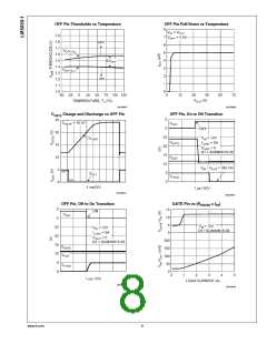
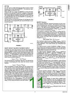
OFF PIN
The OFF pin is a logic level input pin that is used to control
the gate drive to the external MOSFET. The maximum oper-
ating voltage on this pin is 5.5V.
When the OFF pin is high, the MOSFET is turned off (inde-
pendent of the sensed IN and OUT voltages). In this mode,
load current will flow through the body diode of the MOSFET.
The voltage difference between the IN pin and OUT pins will
be approximately 700 mV if the MOSFET is operating nor-
mally through the body diode.
30104824
The OFF pin has an internal pull-down of 5 µA (typical). If the
OFF function is not required the pin may be left open or con-
nected to ground.
FIGURE 8.
MOSFET Selection
The important MOSFET electrical parameters are the maxi-
mum continuous Drain current ID, the maximum Source cur-
rent (i.e. body diode) IS, the maximum drain-to-source voltage
VDS(MAX), the gate-to-source threshold voltage VGS(TH), the
drain-to-source reverse breakdown voltage V(BR)DSS, and the
drain-to-source On resistance RDS(ON)
.
The maximum continuous drain current, ID, rating must ex-
ceed the maximum continuous load current. The rating for the
maximum current through the body diode, IS, is typically rated
the same as, or slightly higher than the drain current, but body
diode current only flows while the MOSFET gate is being
charged to VGS(TH)
.
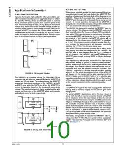
Gate Charge Time = Qg / IGATE(ON)
The maximum drain-to-source voltage, VDS(MAX), must be
high enough to withstand the highest differential voltage seen
in the application. This would include any anticipated fault
conditions.
30104823
FIGURE 7.
The drain-to-source reverse breakdown voltage, V(BR)DSS
,
may provide some transient protection to the OUT pin in low
voltage applications by allowing conduction back to the IN pin
during positive transients at the OUT pin.
SHORT CIRCUIT FAILURE OF AN INPUT SUPPLY
An abrupt zero ohm short circuit across the input supply will
cause the highest possible reverse current to flow while the
internal LM5050-1 control circuitry discharges the gate of the
MOSFET. During this time, the reverse current is limited only
by the RDS(ON) of the MOSFET, along with parasitic wiring re-
sistances and inductances. Worst case instantaneous re-
verse current would be limited to:
The gate-to-source threshold voltage, VGS(TH), should be
compatible with the LM5050-1 gate drive capabilities. Logic
level MOSFETs, with RDS(ON) rated at VGS(TH) at 5V, are rec-
ommended, but sub-Logic level MOSFETs having RDS(ON)
rated at VGS(TH) at 2.5V, can also be used. Standard level
MOSFETs, with RDS(ON) rated at VGS(TH) at 10V, are not rec-
ommended.
ID(REV) = (VOUT - VIN) / RDS(ON)
The dominate MOSFET loss for the LM5050-1 active OR-ing
controller is conduction loss due to source-to-drain current to
the output load, and the RDS(ON) of the MOSFET. This con-
duction loss could be reduced by using a MOSFET with the
lowest possible RDS(ON). However, contrary to popular belief,
arbitrarily selecting a MOSFET based solely on having low
RDS(ON) may not always give desirable results for several rea-
sons:
The internal Reverse Comparator will react, and will start the
process of discharging the Gate, when the reverse current
reaches:
ID(REV) = VSD(REV) / RDS(ON)
When the MOSFET is finally switched off, the energy stored
in the parasitic wiring inductances will be transferred to the
rest of the circuit. As a result, the LM5050-1 IN pin will see a
negative voltage spike while the OUT pin will see a positive
voltage spike. The IN pin can be protected by diode clamping
the pin to GND in the negative direction. The OUT pin can be
protected with a TVS protection diode, a local bypass capac-
itor, or both. In low voltage applications, the MOSFET drainto-
source breakdown voltage rating may be adequate to protect
the OUT pin (i.e. VIN + V(BR)DSS(MAX) < 75V ), but most MOS-
FET datasheets do not guarantee the maximum breakdown
rating, so this method should be used with caution.
1) Reverse transition detection. Higher RDS(ON) will provide
increased voltage information to the LM5050-1 Reverse
Comparator at a lower reverse current level. This will give an
earlier MOSFET turn-off condition should the input voltage
become shorted to ground. This will minimize any disturbance
of the redundant bus.
2) Reverse current leakage. In cases where multiple input
supplies are closely matched it may be possible for some
small current to flow continuously through the MOSFET drain
to source (i.e. reverse) without activating the LM5050-1 Re-
verse Comparator. Higher RDS(ON) will reduce this reverse
current level.
3) Cost. Generally, as the RDS(ON) rating goes lower, the cost
of the MOSFET goes higher.
11
www.ti.com

 TI [ TEXAS INSTRUMENTS ]