LM3886
SNAS091C –MAY 1999–REVISED MARCH 2013
www.ti.com
(1)(2)
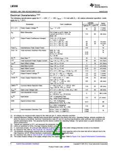
Electrical Characteristics
The following specifications apply for V+ = +28V, V− = −28V, IMUTE = −0.5 mA with RL = 4Ω unless otherwise specified. Limits
apply for TA = 25°C.
LM3886
Units
(Limits)
Parameter
Test Conditions
pin7 − V− ≥ 9V
(3)
(4)
Typical
Limit
|V+| + |V−|
AM
Power Supply Voltage
V
20
84
V (min)
V (max)
(5)
18
Mute Attenuation
Pin 8 Open or at 0V, Mute: On
Current out of Pin 8 > 0.5 mA,
Mute: Off
115
80
dB (min)
(6)
PO
Output Power (Continuous Average)
THD + N = 0.1% (max)
f = 1 kHz; f = 20 kHz
|V+| = |V−| = 28V, RL = 4Ω
|V+| = |V−| = 28V, RL = 8Ω
|V+| = |V−| = 35V, RL = 8Ω
68
38
50
60
30
W (min)
W (min)
W
Peak PO
THD + N
Instantaneous Peak Output Power
Total Harmonic Distortion Plus Noise
135
W
60W, RL = 4Ω,
30W, RL = 8Ω,
20 Hz ≤ f ≤ 20 kHz
AV = 26 dB
%
%
0.03
0.03
(6)
(7)
SR
I+(6)
Slew Rate
VIN = 2.0Vp-p, tRISE = 2 ns
VCM = 0V, Vo = 0V, Io = 0A
VCM = 0V, Io = 0 mA
19
50
8
85
10
1
V/μs (min)
mA (max)
mV (max)
μA (max)
μA (max)
A (min)
Total Quiescent Power Supply Current
Input Offset Voltage
(8)
VOS
1
IB
Input Bias Current
VCM = 0V, Io = 0 mA
0.2
0.01
11.5
IOS
Io
Input Offset Current
VCM = 0V, Io = 0 mA
|V+| = |V−| = 20V, tON = 10 ms, VO = 0V
0.2
7
Output Current Limit
|V+–VO|, V+ = 28V, Io = +100 mA
1.6
2.5
2.0
3.0
V (max)
V (max)
(8)
(9)
Vod
Output Dropout Voltage
|VO–V−|, V− = −28V, Io = −100 mA
(8)
PSRR
Power Supply Rejection Ratio
V+ = 40V to 20V, V− = −40V,
VCM = 0V, Io = 0 mA
120
85
dB (min)
V+ = 40V, V− = −40V to −20V,
VCM = 0V, Io = 0 mA
105
85
dB (min)
(8)
CMRR
Common Mode Rejection Ratio
V+ = 60V to 20V, V− = −20V to −60V,
VCM = 20V to −20V, Io = 0 mA
110
115
8
85
90
2
dB (min)
dB (min)
(8)
AVOL
Open Loop Voltage Gain
Gain-Bandwidth Product
|V+| = |V−| = 28V, RL = 2 kΩ, ΔVO = 40V
|V+| = |V−| = 30V
GBWP
MHz (min)
fO = 100 kHz, VIN = 50 mVrms
(6)
eIN
Input Noise
IHF—A Weighting Filter
2.0
92.5
110
10
μV (max)
RIN = 600Ω (Input Referred)
SNR
IMD
Signal-to-Noise Ratio
PO = 1W, A-Weighted,
Measured at 1 kHz, RS = 25Ω
dB
dB
%
PO = 60W, A-Weighted,
Measured at 1 kHz, RS = 25Ω
Intermodulation Distortion Test
60 Hz, 7 kHz, 4:1 (SMPTE)
60 Hz, 7 kHz, 1:1 (SMPTE)
0.004
0.009
(1) All voltages are measured with respect to the GND pin (pin 7), unless otherwise specified.
(2) Absolute Maximum Ratings indicate limits beyond which damage to the device may occur. Operating Ratings indicate conditions for
which the device is functional. Electrical Characteristics state DC and AC electrical specifications under particular test conditions and
specific performance limits. This assumes that the device is within the Operating Ratings. The typical value is a good indication of
device performance.
(3) Typicals are measured at 25°C and represent the parametric norm.
(4) Limits are speficied to AOQL (Average Outgoing Quality Level).
(5) V− must have at least −9V at its pin with reference to ground in order for the under-voltage protection circuitry to be disabled.
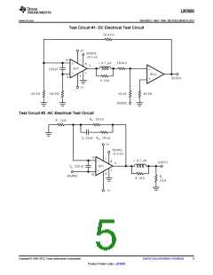
(6) AC Electrical Test; refer to Test Circuit #2 -AC Electrical Test Circuit.
(7) The feedback compensation network limits the bandwidth of the closed-loop response and so the slew rate will be reduced due to the
high frequency roll-off. Without feedback compensation, the slew rate is typically larger.
(8) DC Electrical Test; refer to Test Circuit #1- DC Electrical Test Circuit.
(9) The output dropout voltage is the supply voltage minus the clipping voltage. Refer to Figure 14 in Typical Performance Characteristics.
4
Submit Documentation Feedback
Copyright © 1999–2013, Texas Instruments Incorporated
Product Folder Links: LM3886

 TI [ TEXAS INSTRUMENTS ]