LM3881
SNVS555C –JANUARY 2008–REVISED APRIL 2013
www.ti.com
APPLICATION INFORMATION
OVERVIEW
The LM3881 Power Sequencer provides a simple solution for sequencing multiple rails in a controlled manner. A
clock signal is established that facilitates control of the power up and power down of three open drain FET output
flags. These flags permit connection to shutdown or enable pins of linear regulators and/or switching regulators
to control the power supplies’ operation. This allows a complete power system to be designed without worrying
about large in-rush currents or latch-up conditions that can occur during an uncontrolled startup. An invert (INV)
pin is provided that reverses the logic of the output flags. This pin should be tied to a logic output high or low and
not allowed to remain open circuit. The following discussion assumes the INV pin is held low such that the flag
output is active high.
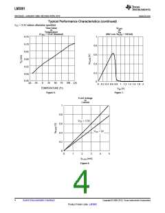
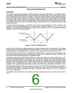
A small external timing capacitor is connected to the TADJ pin that establishes the clock waveform. This
capacitor is linearly charged/discharged by a fixed current source/sink, denoted ITADJ_SRC / ITADJ_SNK, of
magnitude 12 µA between pre-defined voltage threshold levels, denoted VLTH and VHTH, to generate the timing
waveform as shown in the following diagram.
High Threshold Level,
V
H = 1.22V
HT
TADJ
Low Threshold Level,
= 0.5V
V
LTH
T
CLK
Figure 9. TADJ Pin Timing Waveform
Thus, the clock cycle duration is directly proportional to the timing capacitor value. Considering the TADJ voltage
threshold levels and the charge/discharge current magnitude, it can be shown that the timing capacitor-clock
period relationship is typically 120 µs/nF. For example, a 10 nF capacitor sets up a clock period of 1.2 ms.
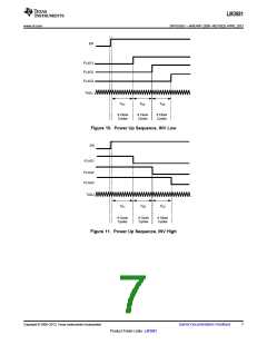
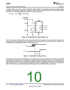
The timing sequence of the LM3881 is controlled by the enable (EN) pin. Upon power up, all the flags are held
low until the precision enable pin exceeds its threshold. After the EN pin is asserted, the power up sequence will
commence and the open-drain flags will be sequentially released.
An internal counter will delay the first flag (FLAG1) from rising until a fixed time period, denoted by TD1 in the
following timing diagram, elapses. This corresponds to at least nine, maximum ten, clock cycles depending on
where EN is asserted relative to the clock signal. Upon release of the first flag, another timer will begin to delay
the release of the second flag (FLAG2). This time delay, denoted TD2, corresponds to exactly eight clock periods.
Similarly, FLAG3 is released after time delay TD3, again eight clock cycles, has expired. Accordingly, a TADJ
capacitor of 10 nF generates typical time delays TD2 and TD3 of 9.6 ms and TD1 of between 10.8 ms and 12.0 ms.
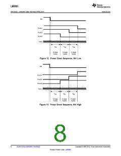
The power down sequence is the same as power up, but in reverse order. When the EN pin is de-asserted, a
timer will begin that delays the third flag (FLAG3) from pulling low. The second and first flag will then follow in a
sequential manner after their appropriate time delays. These time delays, denoted TD4, TD5, TD6, are equal to
TD1, TD2, TD3, respectively.
For robustness, the pull down FET associated with each flag is designed such that it can sustain a short circuit to
VCC.
6
Submit Documentation Feedback
Copyright © 2008–2013, Texas Instruments Incorporated
Product Folder Links: LM3881

 TI [ TEXAS INSTRUMENTS ]