LM3881
SNVS555C –JANUARY 2008–REVISED APRIL 2013
www.ti.com
These devices have limited built-in ESD protection. The leads should be shorted together or the device placed in conductive foam
during storage or handling to prevent electrostatic damage to the MOS gates.
Absolute Maximum Ratings(1)(2)
VCC, EN, INV, TADJ, FLAG1, FLAG2, FLAG3 to GND
-0.3V to +6.0V
-65°C to +150°C
150°C
Storage Temperature Range
Junction Temperature
Lead Temperature (Soldering, 5 sec.)
260°C
(3)
Minimum ESD Rating
2 kV
(1) Absolute Maximum Ratings indicate limits beyond which damage to the device may occur. Operating Ratings indicate conditions for
which the device is intended to be functional, but does not ensure specific performance limits. For ensured specifications and conditions,
see the Electrical Characteristics.
(2) If Military/Aerospace specified devices are required, please contact the Texas Instruments Sales Office/Distributors for availability and
specifications.
(3) The human body model is a 100 pF capacitor discharged through a 1.5 kΩ resistor into each pin.
Operating Ratings(1)
VCC to GND
2.7V to 5.5V
-0.3V to VCC + 0.3V
-40°C to +125°C
EN, INV, TADJ, FLAG1, FLAG2, FLAG3 to GND
Junction Temperature
(1) Absolute Maximum Ratings indicate limits beyond which damage to the device may occur. Operating Ratings indicate conditions for
which the device is intended to be functional, but does not ensure specific performance limits. For ensured specifications and conditions,
see the Electrical Characteristics.
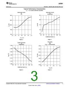
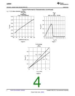
Electrical Characteristics
Specifications with standard typeface are for TJ = 25°C, and those in bold face type apply over the full Operating Temperature
Range (TJ = -40°C to +125°C). Minimum and Maximum limits are ensured through test, design or statistical correlation.
Typical values represent the most likely parametric norm at TJ = 25°C and are provided for reference purposes only. VCC
=
3.3V, unless otherwise specified.
Symbol
IQ
Parameter
Conditions
Min(1)
Typ(2)
Max(1)
110
Unit
Operating Quiescent Current
80
µA
Open Drain Flags
IFLAG
FLAGx Leakage Current
VFLAGx = 3.3V
IFLAGx = 1.2 mA
0.001
1
µA
V
VOL
FLAGx Output Voltage Low
0.4
Time Delays
ITADJ_SRC
ITADJ_SNK
VHTH
TADJ Source Current
TADJ Sink Current
High Threshold Level
Low Threshold Level
Clock Cycle
4
12
12
20
20
µA
µA
V
4
1.0
0.3
1.22
0.5
1.2
1.4
0.7
VLTH
V
TCLK
CADJ = 10 nF
ms
TD1, TD4
Flag Time Delay
9
10
Clock
Cycles
TD2, TD3, TD5, TD6
Flag Time Delay
8
Clock
Cycles
ENABLE Pin
VEN
EN Pin Threshold
1.0
1.22
7
1.5
V
IEN
EN Pin Pull-up Current
VEN = 0V
µA
INV Pin
VIH_INV
VIL_INV
Invert Pin VIH
Invert Pin VIL
90% VCC
V
V
10%
VCC
(1) Limits are 100% production tested at 25°C. Limits over the operating temperature range are ensured through correlation using Statistical
Quality Control (SQC) methods. The limits are used to calculate TI's Average Outgoing Quality Level (AOQL).
(2) Typical numbers are at 25°C and represent the most likely parametric norm.
2
Submit Documentation Feedback
Copyright © 2008–2013, Texas Instruments Incorporated
Product Folder Links: LM3881

 TI [ TEXAS INSTRUMENTS ]