LM2703
SNVS172F –FEBRUARY 2002–REVISED MAY 2013
www.ti.com
LAYOUT CONSIDERATIONS
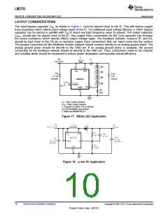
The input bypass capacitor CIN, as shown in Figure 1, must be placed close to the IC. This will reduce copper
trace resistance which effects input voltage ripple of the IC. For additional input voltage filtering, a 100nF bypass
capacitor can be placed in parallel with CIN to shunt any high frequency noise to ground. The output capacitor,
COUT, should also be placed close to the IC. Any copper trace connections for the Cout capacitor can increase
the series resistance, which directly effects output voltage ripple. The feedback network, resistors R1 and R2,
should be kept close to the FB pin to minimize copper trace connections that can inject noise into the system.
The ground connection for the feedback resistor network should connect directly to an analog ground plane. The
analog ground plane should tie directly to the GND pin. If no analog ground plane is available, the ground
connection for the feedback network should tie directly to the GND pin. Trace connections made to the inductor
and schottky diode should be minimized to reduce power dissipation and increase overall efficiency.
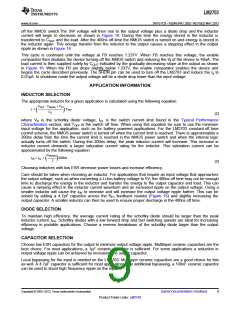
L
V
IN
D
10 mH
2.5V-4.2V
5
1
SW
V
IN
C
IN
C
OUT
4.7 mF
Ceramic
1 mF
Ceramic
LM2703
SHDN
>1.1V
4
0V
3
FB
GND
2
R2
82W
CIN: Taiyo Yuden Ceramic
COUT: Taiyo Yuden Ceramic
L: Coilcraft DT1608C-103 or Murata
LQY33PN100M02 (low profile)
D: Motorola MBRM130LT3
Figure 17. White LED Application
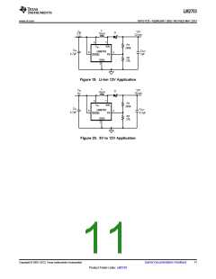
Figure 18. Li-Ion 5V Application
10
Submit Documentation Feedback
Copyright © 2002–2013, Texas Instruments Incorporated
Product Folder Links: LM2703

 TI [ TEXAS INSTRUMENTS ]