LM2672
www.ti.com
SNVS136K –SEPTEMBER 1998–REVISED APRIL 2013
LM2672 Series Buck Regulator Design Procedure (Adjustable Output)
PROCEDURE (Adjustable Output Voltage Version)
EXAMPLE (Adjustable Output Voltage Version)
To simplify the buck regulator design procedure, Texas Instruments
is making available computer design software to be used with the
SIMPLE SWITCHERline of switching regulators.LM267X Made
Simple version 6.0 is available onWindows3.1, NT, or 95 operating
systems.
Given:
Given:
VOUT = 20V
VOUT = Regulated Output Voltage
VIN(max) = Maximum Input Voltage
ILOAD(max) = Maximum Load Current
F = Switching Frequency (Fixed at a nominal 260 kHz).
VIN(max) = 28V
ILOAD(max) = 1A
F = Switching Frequency (Fixed at a nominal 260 kHz).
1. Programming Output Voltage (Selecting R1 and R2, as shown in 1. Programming Output Voltage (Selecting R1 and R2, as shown in
Figure 23)
Figure 23)
Use the following formula to select the appropriate resistor values.
Select R1 to be 1 kΩ, 1%. Solve for R2.
where VREF = 1.21V
(3)
(4)
Select a value for R1 between 240Ω and 1.5 kΩ. The lower resistor
R2 = 1 kΩ (16.53 − 1) = 15.53 kΩ, closest 1% value is 15.4 kΩ.
values minimize noise pickup in the sensitive feedback pin. (For the R2 = 15.4 kΩ.
lowest temperature coefficient and the best stability with time, use
1% metal film resistors.)
(5)
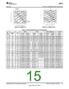
2. Inductor Selection (L1)
2. Inductor Selection (L1)
A. Calculate the inductor Volt • microsecond constant E • T (V • μs), A. Calculate the inductor Volt • microsecond constant (E • T),
from the following formula:
(6)
(7)
where VSAT=internal switch saturation voltage=0.25V and VD = diode
forward voltage drop = 0.5V
B. Use the E • T value from the previous formula and match it with
the E • T number on the vertical axis of the Inductor Value Selection
Guide shown in Figure 27.
B. E • T = 21.6 (V • μs)
C. ILOAD(max) = 1A
C. On the horizontal axis, select the maximum load current.
D. Identify the inductance region intersected by the E • T value and
the Maximum Load Current value. Each region is identified by an
inductance value and an inductor code (LXX).
D. From the inductor value selection guide shown in Figure 27, the
inductance region intersected by the 21.6 (V • μs) horizontal line and
the 1A vertical line is 68 μH, and the inductor code is L30.
E. Select an appropriate inductor from the four manufacturer's part
numbers listed in Table 1. For information on the different types of
inductors, see the inductor selection in the fixed output voltage
design procedure.
E. From the table in Table 1, locate line L30, and select an inductor
part number from the list of manufacturers' part numbers.
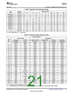
3. Output Capacitor SeIection (COUT
)
3. Output Capacitor SeIection (COUT)
A. Select an output capacitor from the capacitor code selection guide A. Use the appropriate row of the capacitor code selection guide, in
in Table 9. Using the inductance value found in the inductor
selection guide, step 1, locate the appropriate capacitor code
corresponding to the desired output voltage.
Table 9. For this example, use the 15–20V row. The capacitor code
corresponding to an inductance of 68 μH is C20.
Copyright © 1998–2013, Texas Instruments Incorporated
Submit Documentation Feedback
19
Product Folder Links: LM2672

 TI [ TEXAS INSTRUMENTS ]