LM2672
www.ti.com
SNVS136K –SEPTEMBER 1998–REVISED APRIL 2013
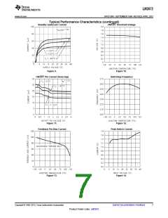
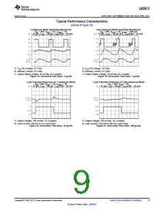
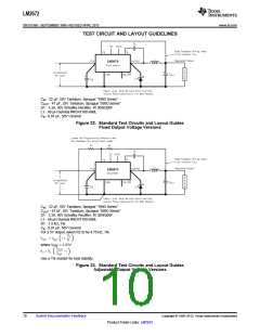
Applications Hints
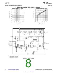
The LM2672 provides all of the active functions required for a step-down (buck) switching regulator. The internal
power switch is a DMOS power MOSFET to provide power supply designs with high current capability, up to 1A,
and highly efficient operation.
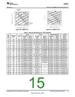
The LM2672 is part of the SIMPLE SWITCHER family of power converters. A complete design uses a minimum
number of external components, which have been pre-determined from a variety of manufacturers. Using either
this data sheet or TI's WEBENCH® design tool, a complete switching power supply can be designed quickly.
Also, refer to the LM2670 data sheet for additional applications information.
SWITCH OUTPUT
This is the output of a power MOSFET switch connected directly to the input voltage. The switch provides energy
to an inductor, an output capacitor and the load circuitry under control of an internal pulse-width-modulator
(PWM). The PWM controller is internally clocked by a fixed 260kHz oscillator. In a standard step-down
application the duty cycle (Time ON/Time OFF) of the power switch is proportional to the ratio of the power
supply output voltage to the input voltage. The voltage on the VSW pin cycles between Vin (switch ON) and below
ground by the voltage drop of the external Schottky diode (switch OFF).
INPUT
The input voltage for the power supply is connected to the VIN pin. In addition to providing energy to the load the
input voltage also provides bias for the internal circuitry of the LM2672. For ensured performance the input
voltage must be in the range of 6.5V to 40V. For best performance of the power supply the VIN pin should always
be bypassed with an input capacitor located close to this pin and GND.
C BOOST
A capacitor must be connected from the CB pin to the VSW pin. This capacitor boosts the gate drive to the internal
MOSFET above Vin to fully turn it ON. This minimizes conduction losses in the power switch to maintain high
efficiency. The recommended value for C Boost is 0.01μF.
GROUND
This is the ground reference connection for all components in the power supply. In fast-switching, high-current
applications such as those implemented with the LM2672, it is recommended that a broad ground plane be used
to minimize signal coupling throughout the circuit
SYNC
This input allows control of the switching clock frequency. If left open-circuited the regulator will be switched at
the internal oscillator frequency, typically 260 kHz. An external clock can be used to force the switching
frequency and thereby control the output ripple frequency of the regulator. This capability provides for consistent
filtering of the output ripple from system to system as well as precise frequency spectrum positioning of the ripple
frequency which is often desired in communications and radio applications. This external frequency must be
greater than the LM2672 internal oscillator frequency, which could be as high as 275 kHz, to prevent an
erroneous reset of the internal ramp oscillator and PWM control of the power switch. The ramp oscillator is reset
on the positive going edge of the sync input signal. It is recommended that the external TTL or CMOS compatible
clock (between 0V and a level greater than 3V) be ac coupled to the SYNC pin through a 100pF capacitor and a
1KΩ resistor to ground.
When the SYNC function is used, current limit frequency foldback is not active. Therefore, the device may not be
fully protected against extreme output short circuit conditions.
FEEDBACK
This is the input to a two-stage high gain amplifier, which drives the PWM controller. Connect the FB pin directly
to the output for proper regulation. For the fixed output devices (3.3V, 5V and 12V outputs), a direct wire
connection to the output is all that is required as internal gain setting resistors are provided inside the LM2672.
For the adjustable output version two external resistors are required to set the dc output voltage. For stable
operation of the power supply it is important to prevent coupling of any inductor flux to the feedback input.
Copyright © 1998–2013, Texas Instruments Incorporated
Submit Documentation Feedback
11
Product Folder Links: LM2672

 TI [ TEXAS INSTRUMENTS ]