AC Electrical Characteristic (Note 5) (Continued)
Symbol
Parameter
Conditions
LF411A
Typ
LF411
Typ
Units
Min
Max Min
Max
<
<
0.02
THD
Total Harmonic Distortion
AV=+10, RL=10k,
VO=20 Vp-p,
0.02
%
BW=20 Hz−20 kHz
Note 1: “Absolute Maximum Ratings” indicate limits beyond which damage to the device may occur. Operating Ratings indicate conditions for which the device is
functional, but do not guarantee specific performance limits.
Note 2: Unless otherwise specified the absolute maximum negative input voltage is equal to the negative power supply voltage.
Note 3: For operating at elevated temperature, these devices must be derated based on a thermal resistance of θ A.
j
Note 4: These devices are available in both the commercial temperature range 0˚C≤T ≤70˚C and the military temperature range −55˚C≤T ≤125˚C. The
A
A
temperature range is designated by the position just before the package type in the device number. A “C” indicates the commercial temperature range and an “M”
indicates the military temperature range. The military temperature range is available in “H” package only.
Note 5: Unless otherwise specified, the specifications apply over the full temperature range and for V = 20V for the LF411A and for V = 15V for the LF411. V ,
OS
S
S
I , and I
are measured at V =0.
B
OS
CM
Note 6: The LF411A is 100% tested to this specification. The LF411 is sample tested to insure at least 90% of the units meet this specification.
Note 7: The input bias currents are junction leakage currents which approximately double for every 10˚C increase in the junction temperature, T . Due to limited
j
production test time, the input bias currents measured are correlated to junction temperature. In normal operation the junction temperature rises above the ambient
temperature as a result of internal power dissipation, P . T =T +θ
P
where θ is the thermal resistance from junction to ambient. Use of a heat sink is
D jA
D
j
A
jA
recommended if input bias current is to be kept to a minimum.
Note 8: Supply voltage rejection ratio is measured for both supply magnitudes increasing or decreasing simultaneously in accordance with common practice, from
15V to 5V for the LF411 and from 20V to 5V for the LF411A.
Note 9: RETS 411X for LF411MH and LF411MJ military specifications.
Note 10: Max. Power Dissipation is defined by the package characteristics. Operating the part near the Max. Power Dissipation may cause the part to operate
outside guaranteed limits.
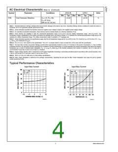
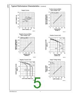
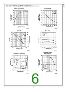
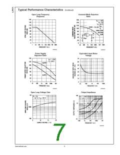
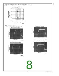
Typical Performance Characteristics
Input Bias Current
Input Bias Current
00565511
00565512
3
www.national.com

 TI [ TEXAS INSTRUMENTS ]