August 2000
LF411
Low Offset, Low Drift JFET Input Operational Amplifier
General Description
Features
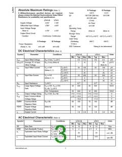
n Internally trimmed offset voltage:
n Input offset voltage drift:
n Low input bias current:
n Low input noise current:
n Wide gain bandwidth:
n High slew rate:
0.5 mV(max)
10 µV/˚C(max)
50 pA
These devices are low cost, high speed, JFET input opera-
tional amplifiers with very low input offset voltage and guar-
anteed input offset voltage drift. They require low supply
current yet maintain a large gain bandwidth product and fast
slew rate. In addition, well matched high voltage JFET input
devices provide very low input bias and offset currents. The
LF411 is pin compatible with the standard LM741 allowing
designers to immediately upgrade the overall performance of
existing designs.
√
0.01 pA/ Hz
3 MHz(min)
10V/µs(min)
1.8 mA
n Low supply current:
n High input impedance:
n Low total harmonic distortion:
n Low 1/f noise corner:
n Fast settling time to 0.01%:
1012
Ω
≤0.02%
50 Hz
2 µs
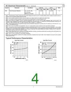
These amplifiers may be used in applications such as high
speed integrators, fast D/A converters, sample and hold
circuits and many other circuits requiring low input offset
voltage and drift, low input bias current, high input imped-
ance, high slew rate and wide bandwidth.
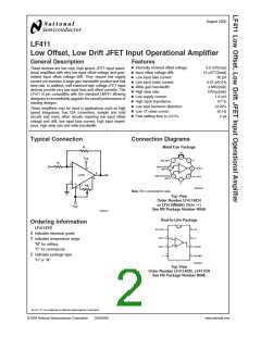
Typical Connection
Connection Diagrams
Metal Can Package
00565505
Note: Pin 4 connected to case.
Top View
Order Number LF411ACH
or LF411MH/883 (Note 11)
See NS Package Number H08A
00565501
Dual-In-Line Package
Ordering Information
LF411XYZ
X indicates electrical grade
Y indicates temperature range
“M” for military
“C” for commercial
Z indicates package type
“H” or “N”
00565507
Top View
Order Number LF411ACN, LF411CN
See NS Package Number N08E
™
BI-FET II is a trademark of National Semiconductor Corporation.
© 2004 National Semiconductor Corporation
DS005655
www.national.com

 TI [ TEXAS INSTRUMENTS ]