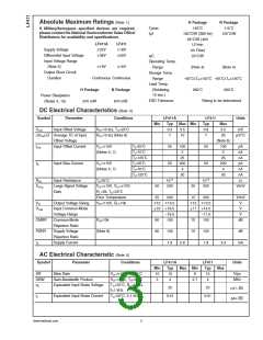
Absolute Maximum Ratings (Note 1)
H Package
150˚C
N Package
115˚C
Tjmax
If Military/Aerospace specified devices are required,
please contact the National Semiconductor Sales Office/
Distributors for availability and specifications.
θjA
162˚C/W (Still Air)
65˚C/W (400
LF/min
120˚C/W
LF411A
22V
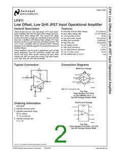
LF411
18V
Supply Voltage
Differential Input Voltage
Input Voltage Range
(Note 2)
Air Flow)
38V
30V
θjC
20˚C/W
Operating Temp.
Range
19V
15V
(Note 4)
(Note 4)
Output Short Circuit
Duration
Storage Temp.
Range
Continuous Continuous
−65˚C≤TA≤150˚C −65˚C≤TA≤150˚C
260˚C 260˚C
Rating to be determined.
Lead Temp.
(Soldering,
10 sec.)
H Package
670 mW
N Package
Power Dissipation
ESD Tolerance
(Notes 3, 10)
670 mW
DC Electrical Characteristics (Note 5)
Symbol
Parameter
Conditions
LF411A
LF411
Typ
Units
Min
Typ
0.3
7
Max Min
Max
2.0
VOS
Input Offset Voltage
RS=10 kΩ, TA=25˚C
RS=10 kΩ (Note 6)
0.5
10
0.8
7
mV
∆VOS/∆T Average TC of Input
20
µV/˚C
Offset Voltage
(Note 6)
100
2
IOS
Input Offset Current
VS= 15V
Tj=25˚C
Tj=70˚C
Tj=125˚C
Tj=25˚C
Tj=70˚C
Tj=125˚C
25
50
100
2
25
50
pA
nA
(Notes 5, 7)
25
200
4
25
nA
IB
Input Bias Current
VS= 15V
200
4
pA
(Notes 5, 7)
nA
50
50
nA
RIN
Input Resistance
Large Signal Voltage
Gain
Tj=25˚C
1012
200
1012
200
Ω
AVOL
VS= 15V, VO= 10V,
RL=2k, TA=25˚C
Over Temperature
VS= 15V, RL=10k
50
25
V/mV
25
12
200
15
12
200
V/mV
V
VO
Output Voltage Swing
Input Common-Mode
Voltage Range
13.5
13.5
VCM
16 +19.5
−16.5
11 +14.5
−11.5
V
V
CMRR
PSRR
IS
Common-Mode
Rejection Ratio
Supply Voltage
RS≤10k
80
100
100
1.8
70
100
100
1.8
dB
(Note 8)
80
70
dB
Rejection Ratio
Supply Current
2.8
3.4
mA
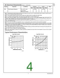
AC Electrical Characteristic (Note 5)
Symbol
Parameter
Conditions
LF411A
LF411
Typ
15
Units
Min
10
3
Typ
15
4
Max Min
Max
SR
Slew Rate
VS= 15V, TA=25˚C
VS= 15V, TA=25˚C
TA=25˚C, RS=100Ω,
f=1 kHz
8
V/µs
MHz
GBW
en
Gain-Bandwidth Product
2.7
4
Equivalent Input Noise Voltage
25
25
in
Equivalent Input Noise Current
TA=25˚C, f=1 kHz
0.01
0.01
www.national.com
2

 TI [ TEXAS INSTRUMENTS ]