LF155, LF156, LF355, LF356, LF357
SNOSBH0C –MAY 2000–REVISED MARCH 2013
www.ti.com
Units
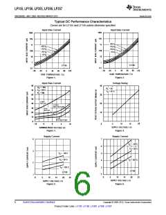
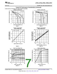
DC Electrical Characteristics
LF256/7
LF356B
LF155/6
Min Typ
LF355/6/7
Max Min Typ Max
Symbol
VOS
Parameter
Conditions
Max Min Typ
Input Offset Voltage
RS=50Ω, TA=25°C
Over Temperature
RS=50Ω
3
5
7
3
5
3
10
13
mV
mV
6.5
ΔVOS/ΔT
ΔTC/ΔVOS
IOS
Average TC of Input
Offset Voltage
5
5
5
μV/°C
(2)
Change in Average TC
with VOS Adjust
RS=50Ω,
μV/°C
per mV
0.5
3
0.5
3
0.5
3
(1) (3)
Input Offset Current
Input Bias Current
Input Resistance
TJ=25°C,
20
20
20
1
50
2
pA
nA
TJ≤THIGH
(1) (3)
IB
TJ=25°C,
30
100
50
30
100
5
30
200
8
pA
TJ≤THIGH
nA
RIN
TJ=25°C
1012
200
1012
200
1012
200
Ω
AVOL
Large Signal Voltage
Gain
VS=±15V, TA=25°C
VO=±10V, RL=2k
Over Temperature
VS=±15V, RL=10k
VS=±15V, RL=2k
VS=±15V
50
50
25
V/mV
25
25
15
V/mV
VO
Output Voltage Swing
±12
±10
±13
±12
±12
±10
±13
±12
±12
±10
±13
±12
V
V
V
V
VCM
Input Common-Mode
Voltage Range
+15.1
−12
±15.1
−12
+15.1
−12
±11
±11
+10
CMRR
PSRR
Common-Mode
Rejection Ratio
85
85
100
100
85
85
100
100
80
80
100
100
dB
dB
(4)
Supply Voltage Rejection
Ratio
(1) Unless otherwise stated, these test conditions apply:
LF155/156
LF256/257
±15V ≤ VS ≤ ±20V
−25°C ≤ TA ≤ +85°C 0°C ≤ TA ≤ +70°C
LF356B
LF355/6/7
VS= ±15V
Supply Voltage, VS
TA
±15V ≤ VS ≤ ±20V
±15V ≤ VS ±20V
−55°C ≤ TA ≤
0°C ≤ TA ≤ +70°C
+125°C
THIGH
+125°C
+85°C
+70°C
+70°C
and VOS, IB and IOS are measured at VCM = 0.
(2) The Temperature Coefficient of the adjusted input offset voltage changes only a small amount (0.5μV/°C typically) for each mV of
adjustment from its original unadjusted value. Common-mode rejection and open loop voltage gain are also unaffected by offset
adjustment.
(3) The input bias currents are junction leakage currents which approximately double for every 10°C increase in the junction temperature,
TJ. Due to limited production test time, the input bias currents measured are correlated to junction temperature. In normal operation the
junction temperature rises above the ambient temperature as a result of internal power dissipation, Pd. TJ = TA + θJA Pd where θJA is
the thermal resistance from junction to ambient. Use of a heat sink is recommended if input bias current is to be kept to a minimum.
(4) Supply Voltage Rejection is measured for both supply magnitudes increasing or decreasing simultaneously, in accordance with common
practice.
DC Electrical Characteristics
TA = TJ = 25°C, VS = ±15V
LF155
LF355
LF156/256/257/356B
LF356
LF357
Parameter
Units
Typ
Max
Typ
Max
Typ
Max
Typ
Max
Typ
Max
Supply
Current
2
4
2
4
5
7
5
10
5
10
mA
4
Submit Documentation Feedback
Copyright © 2000–2013, Texas Instruments Incorporated
Product Folder Links: LF155 LF156 LF355 LF356 LF357

 TI [ TEXAS INSTRUMENTS ]