INA282, INA283
INA284, INA285
INA286
SBOS485A –NOVEMBER 2009–REVISED JULY 2010
www.ti.com
Example 2
INA286; VS = 5V; VCM = 24V; VREF = 0V; VSENSE = 10mV
Table 2. Example 2
TERM
SYMBOL
EQUATION
TYPICAL VALUE
MAXIMUM VALUE
Initial Input Offset
Voltage
VOS
—
20mV
70mV
Added Input Offset
Voltage Because of
Common-Mode
Voltage
1
CMRR_dB
´ (VCM - 12V)
(
VOS_CM
1.2mV
12mV
(
20
10
Added Input Offset
Voltage Because of
Reference Voltage
R
CMR ´ (2.048V - VREF)
VOS_REF
VOS_Total
Error_VOS
34.8mV
40.2mV
0.40%
92.2mV
116.4mV
1.16%
Total Input Offset
Voltage
2
(VOS)2 + (VOS_CM)2 + (VOS_REF
)
VOS_Total
Error from Input
Offset Voltage
´ 100
VSENSE
Gain Error
Error_Gain
Error_Lin
—
—
0.40%
0.01%
1.40%
0.01%
Nonlinearity Error
(Error_VOS)2 + (Error_Gain)2 + (Error_Lin)2
Total Error
—
0.57%
1.82%
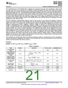
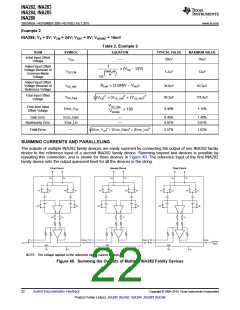
SUMMING CURRENTS AND PARALLELING
The outputs of multiple INA282 family devices are easily summed by connecting the output of one INA282 family
device to the reference input of a second INA282 family device. Summing beyond two devices is possible by
repeating this connection, and is shown for three devices in Figure 40. The reference input of the first INA282
family device sets the output quiescent level for all the devices in the string.
First Circuit
Second Circuit
Third Circuit
VIN+
VIN-
VIN+
VIN-
VIN+
VIN-
Æ1
Æ2
Æ2
Æ1
Æ1
Æ2
Æ2
Æ1
Æ1
Æ2
Æ2
Æ1
Æ2
Æ2
Æ2
Æ2
Æ2
Æ2
Æ1
Æ1
Æ1
Æ1
Output
Output
Output
Summed
Output
VREF
GND
GND
GND
V+
V+
V+
NOTE: The voltage applied to the reference inputs cannot exceed 9V.
Figure 40. Summing the Outputs of Multiple INA282 Family Devices
22
Submit Documentation Feedback
Copyright © 2009–2010, Texas Instruments Incorporated
Product Folder Link(s): INA282 INA283 INA284 INA285 INA286

 TI [ TEXAS INSTRUMENTS ]