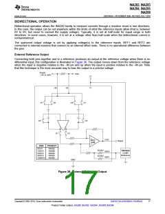
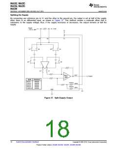
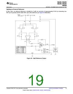
INA282, INA283
INA284, INA285
INA286
www.ti.com
SBOS485A –NOVEMBER 2009–REVISED JULY 2010
The nonlinearity error of the INA282-286 is relatively low compared to the gain error specification, which results
in a gain error that can be expected to be relatively constant throughout the linear input range of the device.
While the gain error remains constant across the linear input range of the device, the error associated with the
input offset voltage does not. As the differential input voltage developed across a shunt resistor at the input of the
INA282-286 decreases, the inherent input offset voltage of the device becomes a larger percentage of the
measured input signal resulting in an increase in error in the measurement. This varying error is present among
all current shunt monitors, given the input offset voltage ratio to the voltage being sensed by the device. The
relatively low input offset voltages present in the INA282-286 devices limit the amount of contribution the offset
voltage has on the total error term.
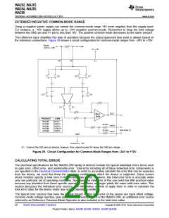
The term Reference Common-Mode Rejection refers to the amount of error induced by applying a reference
voltage to the INA282-286 device that deviates from the inherent bias voltage present at the output of the first
stage of the device. The output of the switched-capacitor network and first-stage amplifier has an inherent bias
voltage of approximately 2.048V. Applying a reference voltage of 2.048V to the INA282-286 reference pins
results in no additional error term contribution. Applying a voltage to the reference pins that differs from 2.048V
creates a voltage potential in the internal difference amplifier, resulting in additional current flowing through the
resistor network. As a result of resistor tolerances, this additional current flow causes additional error at the
output because of resistor mismatches. Additionally, as a result of resistor tolerances, this additional current flow
causes additional error at the output based on the common-mode rejection ratio of the output stage amplifier.
This error term is referred back to the input of the device as additional input offset voltage. Increasing the
difference between the 2.048V internal bias and the external reference voltage results in a higher input offset
voltage. Also, as the error at the output is referred back to the input, there is a larger impact on the input-referred
offset, VOS, for the lower-gain versions of the device.
Two examples are provided that detail how different operating conditions can affect the total error calculations.
Typical and maximum calculations are shown as well to provide the user more information on how much error
variance could be present from device to device.
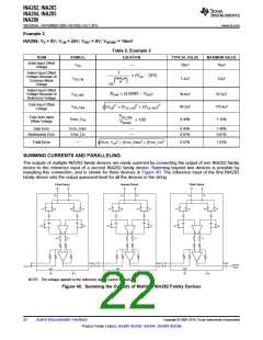
Example 1
INA282; VS = 5V; VCM = 12V; VREF = 2.048V; VSENSE = 10mV
Table 1. Example 1
TERM
SYMBOL
EQUATION
TYPICAL VALUE
MAXIMUM VALUE
Initial Input Offset
Voltage
VOS
—
20mV
70mV
Added Input Offset
Voltage Because of
Common-Mode
Voltage
1
CMRR_dB
´ (VCM - 12V)
(
VOS_CM
0mV
0mV
(
20
10
Added Input Offset
Voltage Because of
Reference Voltage
R
CMR ´ (2.048V - VREF)
VOS_REF
VOS_Total
Error_VOS
0mV
20mV
0.20%
0mV
70mV
0.70%
Total Input Offset
Voltage
2
(VOS)2 + (VOS_CM)2 + (VOS_REF
)
VOS_Total
Error from Input
Offset Voltage
´ 100
VSENSE
Gain Error
Error_Gain
Error_Lin
—
—
0.40%
0.01%
1.40%
0.01%
Nonlinearity Error
(Error_VOS)2 + (Error_Gain)2 + (Error_Lin)2
Total Error
—
0.45%
1.56%
Copyright © 2009–2010, Texas Instruments Incorporated
Submit Documentation Feedback
21
Product Folder Link(s): INA282 INA283 INA284 INA285 INA286

 TI [ TEXAS INSTRUMENTS ]