The maximum differential input voltage for accurate mea-
surements is 0.5V, which produces a 500µA output current.
A differential input voltage of up to 2V will not cause damage.
Differential measurements (pins 3 and 4) must be unipolar
with a more-positive voltage applied to pin 3. If a more-
negative voltage is applied to pin 3, the output current (IO) is
zero, but will not cause damage.
IS
3
4
INA139
ZIN
OPA340
BASIC CONNECTION
RL
Buffer of amp drives the A/D converter
without affecting gain.
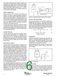
Figure 1 shows the basic connection of the INA139. The
input pins, VIN+ and VIN– , must be connected as closely as
possible to the shunt resistor to minimize any resistance in
series with the shunt resistance. The output resistor, RL, is
shown connected between pin 1 and ground. Best accuracy
is achieved with the output voltage measured directly across
RL. This is especially important in high-current systems
where load current can flow in the ground connections,
affecting the measurement accuracy.
FIGURE 2. Buffering Output to Drive the A/D Converter.
OUTPUT VOLTAGE RANGE
The output of the INA139 is a current that is converted to a
voltage by the load resistor, RL. The output current remains
accurate within the compliance voltage range of the output
circuitry. The shunt voltage and the input common-mode and
power-supply voltages limit the maximum possible output
swing. The maximum output voltage compliance is limited by
the lower of the two equations below:
No power-supply bypass capacitors are required for stability
of the INA139. However, applications with noisy or high-
impedance power supplies can require decoupling capaci-
tors to reject power-supply noise; connect the bypass capaci-
tors close to the device pins.
VOUT MAX = (V+) – 0.7V – (VIN+ – VIN–
or
)
(4)
POWER SUPPLIES
VOUT MAX = (VIN–) – 0.5V
(whichever is lower)
(5)
The input circuitry of the INA139 can accurately measure
beyond its power-supply voltage, V+. For example, the V+
power supply can be 5V whereas the load power-supply
voltage is up to +36V (or +60V with the INA169). However,
the output voltage range of the OUT terminal (pin 1) is limited
by the lesser of the two voltages (see the Output Voltage
Range section).
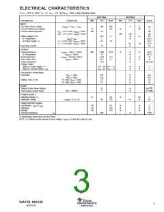
BANDWIDTH
Measurement bandwidth is affected by the value of the load
resistor, RL. High gain produced by high values of RL will
yield a narrower measurement bandwidth (see the Typical
Characteristics). For widest possible bandwidth, keep the
capacitive load on the output to a minimum.
SELECTING RS AND RL
If bandwidth limiting (filtering) is desired, a capacitor can be
added to the output, as shown in Figure 3, which will not
cause instability.
The value chosen for the shunt resistor, RS, depends on the
application and is a compromise between small-signal accu-
racy and maximum permissible voltage loss in the measure-
ment line. High values of RS provide better accuracy at lower
currents by minimizing the effects of offset, whereas low
values of RS minimize voltage loss in the supply line. For most
applications, best performance is attained with an RS value
that provides a full-scale shunt voltage of 50mV to 100mV;
maximum input voltage for accurate measurements is 500mV.
3
4
f–3dB
1
f–3dB
=
INA139
2πRLCL
RL is chosen to provide the desired full-scale output voltage.
The output impedance of the INA139 OUT terminal is very
high, which permits using values of RL up to 100kΩ with
excellent accuracy. The input impedance of any additional
circuitry at the output must be much higher than the value of
RL to avoid degrading accuracy.
VO
CL
RL
FIGURE 3. Output Filter.
Some Analog-to-Digital (A/D) converters have input imped-
ances that will significantly affect measurement gain. The input
impedance of the A/D converter can be included as part of the
effective RL if its input can be modeled as a resistor to ground.
Alternatively, an op amp can be used to buffer the A/D
converter input, as shown in Figure 2, see Figure 1 for
recommended values of RL.
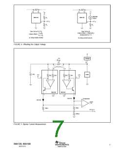
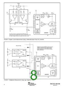
APPLICATIONS
The INA139 is designed for current shunt measurement
circuits (see Figure 1), but its basic function is useful in a
wide range of circuitry. A creative engineer will find many
unforeseen uses in measurement and level shifting circuits.
A few ideas are illustrated in Figures 4 through 7.
INA139, INA169
6
SBOS181D
www.ti.com

 TI [ TEXAS INSTRUMENTS ]