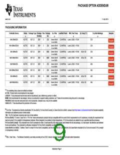
PACKAGE/ORDERING INFORMATION(1)
SPECIFIED
TEMPERATURE
RANGE
PACKAGE
DESIGNATOR
PACKAGE
MARKING
ORDERING
NUMBER
TRANSPORT
MEDIA, QUANTITY
PRODUCT
PACKAGE-LEAD
INA139
SOT23-5 Surface-Mount
DBV
"
–40°C to +85°C
E39
"
INA139NA/250
INA139NA/3K
INA169NA/250
INA169NA/3K
Tape and Reel, 250
Tape and Reel, 3000
Tape and Reel, 250
Tape and Reel, 3000
"
INA169
"
"
"
SOT23-5 Surface-Mount
DBV
–40°C to +85°C
A69
"
"
"
"
NOTE: (1) For the most current package and ordering information, see the Package Option Addendum at the end of this document, or see the TI website at
www.ti.com.
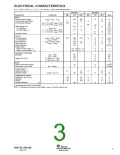
ABSOLUTE MAXIMUM RATINGS(1)
ELECTROSTATIC
DISCHARGE SENSITIVITY
This integrated circuit can be damaged by ESD. Texas Instru-
ments recommends that all integrated circuits be handled with
Supply Voltage, V+
INA139 ............................................................................... –0.3V to 60V
INA169 ............................................................................... –0.3V to 75V
Analog Inputs, VIN+, VIN–
INA139
Common Mode(2) ............................................................ –0.3V to 60V
Differential (VIN+) – (VIN–) .................................................. –40V to 2V
INA169
appropriate precautions. Failure to observe proper handling
and installation procedures can cause damage.
Common Mode(2) ............................................................ –0.3V to 75V
Differential (VIN+) – (VIN–) .................................................. –40V to 2V
Analog Output, Out(2) ........................................................... –0.3V to 40V
Input Current Into Any Pin ............................................................... 10mA
Operating Temperature ..................................................–55°C to +125°C
Storage Temperature .....................................................–65°C to +125°C
Junction Temperature .................................................................... +150°C
ESD damage can range from subtle performance degrada-
tion to complete device failure. Precision integrated circuits
may be more susceptible to damage because very small
parametric changes could cause the device not to meet its
published specifications.
NOTE: (1) Stresses above these ratings may cause permanent damage.
Exposure to absolute maximum conditions for extended periods may degrade
device reliability. These are stress ratings only, and functional operation of the
device at these or any other conditions beyond those specified is not implied.
(2) The input voltage at any pin may exceed the voltage shown if the current
at that pin is limited to 10mA.
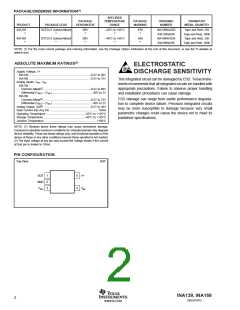
PIN CONFIGURATION
Top View
SOT
OUT
GND
VIN+
1
2
3
5
4
V+
VIN–
INA139, INA169
2
SBOS181D
www.ti.com

 TI [ TEXAS INSTRUMENTS ]