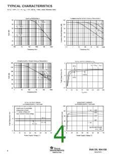
TYPICAL CHARACTERISTICS (Cont.)
At TA = +25°C, V+ = 5V, VIN+ = 12V, and RL = 25kΩ, unless otherwise noted.
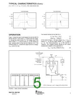
STEP RESPONSE
STEP RESPONSE
1V
1.5V
G = 50
0V
G = 100
0.5V
2V
G = 10
0V
1V
G = 100
0V
10µs/div
20µs/div
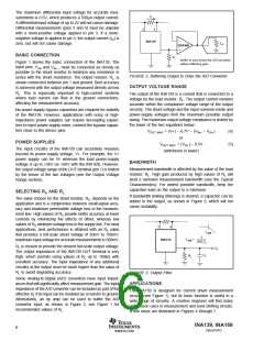
The transfer function for the INA139 is:
OPERATION
IO = gm (VIN+) – (VIN–
)
(1)
(2)
Figure 1 shows the basic circuit diagram for both the INA139
and the INA169. Load current, IS, is drawn from the supply,
VS, through the shunt resistor, RS. The voltage drop in the
shunt resistor, VS, is forced across RG1 by the internal op
amp, causing current to flow into the collector of Q1. The
external resistor, RL, converts the output current to a voltage,
where gm = 1000µA/V
In the circuit of Figure 1, the input voltage, (VIN+) – (VIN–), is
equal to IS • RS and the output voltage, VOUT, is equal to
IO • RL. The transconductance, gm, of the INA139 is
1000µA/V. The complete transfer function for the current
measurement amplifier in this application is:
VOUT, at the OUT pin.
VOUT = (IS) (RS) (1000µA/V) (RL)
(3)
VP
Load Power Supply
+2.7V to 40V(1)
Shunt
RS
IS
VIN+
VIN–
V+ power can be
common or
independent of
3
4
Load
V+
load supply.
RG1
1kΩ
RG2
1kΩ
2.7V ≤ (V+) ≤ 40V(1)
5
Q1
OUT
1
INA139
VOLTAGE GAIN
EXACT RL (Ω)
NEAREST 1% RL (Ω)
+
VO
–
2
IO
1
2
1k
2k
1k
2k
RL
5
5k
4.99k
10k
20k
49k
100k
10
20
50
100
10k
20k
50k
100k
NOTE: (1) Maximum VP and V+ voltage is 60V with the INA169.
FIGURE 1. Basic Circuit Connections.
INA139, INA169
5
SBOS181D
www.ti.com

 TI [ TEXAS INSTRUMENTS ]