DS75176B, DS75176BT
www.ti.com
SNLS381C –JULY 1998–REVISED APRIL 2013
Electrical Characteristics (1) (2) (continued)
0°C ≤ TA≤ 70°C, 4.75V < VCC< 5.25V unless otherwise specified
Symbol
VIH
Parameter
Input High Voltage
Conditions
Min Typ Max Units
2
V
VIL
VCL
IIL
Input Low Voltage
Input Clamp Voltage
Input Low Current
Input High Current
Input Current
0.8
−1.5
−200
20
DI, DE,
RE , E
IIN = −18 mA
VIL = 0.4V
VIH = 2.4V
VIN = 12V
VIN = −7V
μA
μA
IIH
IIN
DO/RI, DO/RI
VCC = 0V or 5.25V
DE = 0V
+1.0
−0.8
mA
mA
VTH
Differential Input Threshold Voltage for
Receiver
−7V ≤ VCM ≤ + 12V
−0.
2
+0.2
V
ΔVTH
VOH
VOL
Receiver Input Hysteresis
VCM = 0V
70
mV
V
Receiver Output High Voltage
IOH = −400 μA
2.7
12
(3)
Output Low Voltage
RO
IOL = 16 mA
0.5
V
IOZR
OFF-State (High Impedance)
Output Current at Receiver
Receiver Input Resistance
Supply Current
VCC = Max
±20
μA
0.4V ≤ VO ≤ 2.4V
−7V ≤ VCM ≤ +12V
No Load(3)
RIN
ICC
kΩ
mA
mA
mA
mA
mA
Driver Outputs Enabled
Driver Outputs Disabled
55
35
(3)
IOSD
Driver Short-Circuit
Output Current
VO = −7V
−250
+250
−85
(3)
VO = +12V
IOSR
Receiver Short-Circuit
Output Current
VO = 0V
−15
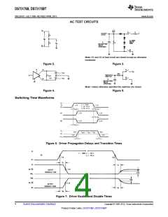
Switching Characteristics
VCC = 5.0V, TA = 25°C
Symbol
tPLH
tPHL
tr
Parameter
Driver Input to Output
Conditions
Min
Typ
12
Max
Units
ns
RLDIFF = 60Ω
22
22
18
18
Driver Input to Output
Driver Rise Time
Driver Fall Time
CL1 = CL2 = 100 pF
RLDIFF = 60Ω
17
ns
ns
tf
CL1 =CL2 = 100 pF
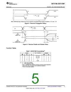
(Figure 4 and Figure 6)
ns
tZH
tZL
tLZ
tHZ
Driver Enable to Output High
Driver Enable to Output Low
Driver Disable Time from Low
Driver Disable Time from High
CL = 100 pF (Figure 5 and Figure 7) S1
Open
29
31
13
19
100
60
ns
ns
ns
ns
CL = 100 pF (Figure 5 and Figure 7) S2
Open
CL = 15 pF (Figure 5 and Figure 7) S2
Open
30
CL = 15 pF (Figure 5 and Figure 7) S1
Open
200
tPLH
tPHL
tZL
Receiver Input to Output
Receiver Input to Output
Receiver Enable to Output Low
CL = 15 pF (Figure 3 and Figure 8)
S1 and S2 Closed
30
32
15
37
37
20
ns
ns
ns
CL = 15 pF (Figure 3 and Figure 9) S2
Open
tZH
tLZ
tHZ
Receiver Enable to Output High
Receiver Disable from Low
Receiver Disable from High
CL = 15 pF (Figure 3 and Figure 9) S1
Open
11
28
13
20
32
35
ns
ns
ns
CL = 15 pF (Figure 3 and Figure 9) S2
Open
CL = 15 pF (Figure 3 and Figure 9) S1
Open
Copyright © 1998–2013, Texas Instruments Incorporated
Submit Documentation Feedback
3
Product Folder Links: DS75176B DS75176BT

 TI [ TEXAS INSTRUMENTS ]