DS75176B, DS75176BT
SNLS381C –JULY 1998–REVISED APRIL 2013
www.ti.com
(1)(2)
Absolute Maximum Ratings
Supply Voltage, VCC
7V
7V
Control Input Voltages
Driver Input Voltage
7V
Driver Output Voltages
+15V/ −10V
+15V/ −10V
5.5V
Receiver Input Voltages (DS75176B)
Receiver Output Voltage
(3)
Continuous Power Dissipation @ 25°C
for SOIC Package
for PDIP Package
675 mW
(4)
900 mW
Storage Temperature Range
−65°C to +150°C
Lead Temperature
(Soldering, 4 seconds)
260°C
500V
ESD Rating (HBM)
(1) “Absolute Maximum Ratings” are those beyond which the safety of the device cannot be verified. They are not meant to imply that the
device should be operated at these limits. The tables of “Electrical Characteristics” provide conditions for actual device operation.
(2) If Military/Aerospace specified devices are required, please contact the TI Sales Office/Distributors for availability and specifications.
(3) Derate linearly @ 6.11 mW/°C to 400 mW at 70°C.
(4) Derate linearly at 5.56 mW/°C to 650 mW at 70°C.
Recommended Operating Conditions
Min
4.75
−7
Max
5.25
+12
Units
Supply Voltage, VCC
V
V
Voltage at Any Bus Terminal
(Separate or Common Mode)
Operating Free Air Temperature TA
DS75176B
0
+70
+85
+12
°C
°C
V
DS75176BT
−40
−12
(1)
Differential Input Voltage, VID
(1) Differential - Input/Output bus voltage is measured at the noninverting terminal A with respect to the inverting terminal B.
(1) (2)
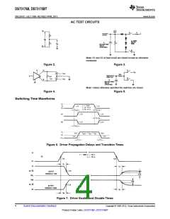
Electrical Characteristics
0°C ≤ TA≤ 70°C, 4.75V < VCC< 5.25V unless otherwise specified
Symbol
Parameter
Conditions
Min Typ Max Units
VOD1
Differential Driver Output
Voltage (Unloaded)
IO = 0
5
V
(3)
VOD2
Differential Driver Output
Voltage (with Load)
See (Figure 2)
R = 50Ω; (RS-422)
R = 27Ω; (RS-485)
2
V
V
1.5
ΔVOD
Change in Magnitude of Driver
Differential Output Voltage For
Complementary Output States
Driver Common Mode Output Voltage
Change in Magnitude of Driver
Common Mode Output Voltage
For Complementary Output States
0.2
V
VOC
See (Figure 2)
R = 27Ω
3.0
0.2
V
V
Δ|VOC
|
(1) All currents into device pins are positive; all currents out of device pins are negative. All voltages are referenced to device ground unless
otherwise specified.
(2) All typicals are given for VCC = 5V and TA = 25°C.
(3) All worst case parameters for which this note is applied, must be increased by 10% for DS75176BT. The other parameters remain valid
for −40°C < TA < +85°C.
2
Submit Documentation Feedback
Copyright © 1998–2013, Texas Instruments Incorporated
Product Folder Links: DS75176B DS75176BT

 TI [ TEXAS INSTRUMENTS ]