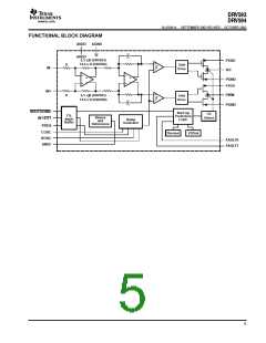
DRV593
DRV594
www.ti.com
SLOS401A - SEPTEMBER 2002 REVISED - OCTOBER 2002
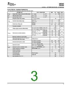
ELECTRICAL CHARACTERISTICS
over operating free-air temperature range unless otherwise noted
PARAMETER
TEST CONDITIONS
= 0 A
MIN
TYP
MAX
100
1
UNIT
mV
µA
|V
|
Output offset voltage (measured differentially)
High-level input current
V = V /2,
I
O
14
OO
I
DD
|I
|
IH
V
DD
V
DD
= 5.5V,
V = V
I DD
|I |
IL
Low-level input current
= 5.5V,
V = 0 V
I
1
µA
Vn
Integrated output noise voltage
f = <1 Hz to 10 kHz
40
µV
V
V
= 5 V
1.2
1.2
3.8
2.1
DD
DD
V
Common-mode voltage range
V
ICM
v
= 3.3 V
DRV593
DRV594
2.1
2.3
14.5
60
2.6
V/V
V/V
kHz
A
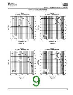
Closed-loop voltage gain
Full power bandwidth
13.7
15.3
I
I
= ±1 A, r
= ±3 A, r
= 65 mΩ,
V = 5 V
DD
4.87
4.61
60
O
ds(on)
V
Voltage output (measured differentially)
V
O
= 65 mΩ, V = 5 V
O
ds(on)
DD
High side
Low side
High side
Low side
25
25
25
25
95
95
V
= 5 V, I = 4 A,
O
DD
mΩ
T = 25°C
65
A
r
Drain-source on-state resistance
Maximum continuous current output
DS(on)
80
140
140
V
= 3.3 V, I = 4 A,
O
DD
mΩ
A
T = 25°C
90
A
3
Status flag output pins (FAULT0, FAULT1)
Fault active (open drain output)
Sinking 200 µA
0.1
V
For 500 kHz operation
For 100 kHz operation
225
45
250
50
4
300
55
12
8
External clock frequency range
Quiescent current
kHz
mA
V
DD
V
DD
V
DD
= 5 V, No load or filter
= 3.3 V, No load or filter
I
I
q
2.5
40
2
Quiescent current in shutdown mode
Output resistance in shutdown
Power-on threshold
= 5 V, SHUTDOWN = 0.8 V
0
1
80
µA
kΩ
V
q(SD)
SHUTDOWN = 0.8 V
1.7
1.6
2.8
2.6
Power-off threshold
V
Thermal trip point
FAULT0 active
Power off
115
150
100
°C
°C
kΩ
Thermal shutdown
Z
I
Input impedance (IN+, IN-)
3

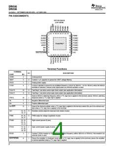
 TI [ TEXAS INSTRUMENTS ]