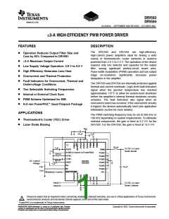
DRV593
DRV594
www.ti.com
SLOS401A - SEPTEMBER 2002 REVISED - OCTOBER 2002
This integrated circuit can be damaged by ESD. Texas
Instruments recommends that all integrated circuits be
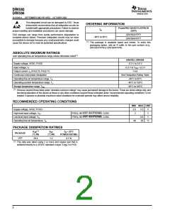
ORDERING INFORMATION
handledwith appropriate precautions. Failure to observe
proper handling and installation procedures can cause damage.
PowerPAD QUAD FLATPACK
(VFP)
T
A
(1)
ESD damage can range from subtle performance degradation to
complete device failure. Precision integrated circuits may be more
susceptible to damage because very small parametric changes could
cause the device not to meet its published specifications.
DRV593VFP
-40°C to 85°C
(1)
DRV594VFP
(1)
This package is available taped and reeled. To order this
packaging option, add an R suffix to the part number (e.g.,
DRV593VFPR or DRV594VFPR).
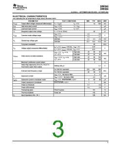
ABSOLUTE MAXIMUM RATINGS
over operating free-air temperature range unless otherwise noted
(1)
DRV593, DRV594
Supply voltage, AVDD, PVDD
-0.3 V to 5.5 V
Input voltage, V
-0.3 V to V + 0.3 V
I
DD
Output current, I (FAULT0, FAULT1)
1 mA
See Dissipation Rating Table
-40°C to 85°C
O
Continuous total power dissipation
Operating free-air temperature range, T
A
Operating junction temperature range, T
-40°C to 150°C
J
Storage temperature range, T
-65°C to 165°C
stg
(1)
Stresses beyond those listed under “absolute maximum ratings” may cause permanent damage to the device. These are stress ratings only, and
functional operation of the device at these or any other conditions beyond those indicated under “recommended operating conditions” is not
implied. Exposure to absolute-maximum-rated conditions for extended periods may affect device reliability.
RECOMMENDED OPERATING CONDITIONS
MIN MAX UNIT
Supply voltage, AVDD PVDD
2.8
2
5.5
V
V
,
High-level input voltage, V
FREQ, INT/EXT, SHUTDOWN, COSC
FREQ, INT/EXT, SHUTDOWN, COSC
IH
Low-level input voltage, V
0.8
85
V
IL
Operating free-air temperature, T
- 40
°C
A
PACKAGE DISSIPATION RATINGS
(1)
Θ
JA
Θ
JC
T = 25°C
A
PACKAGE
(°C/W)
(°C/W)
POWER RATING
VFP
29.4
1.2
4.1 W
(1)
This data was taken using 2 oz trace and copper pad that is
soldered directly to a JEDEC standard 4-layer 3 in × 3 in PCB.
2

 TI [ TEXAS INSTRUMENTS ]