8.0 Electrical Specifications (Continued)
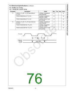
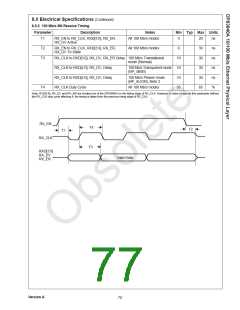
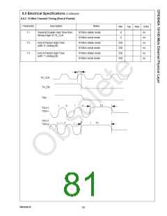
8.5.2 100 Mb/s MII Receive Timing
Parameter
Description
Notes
Min Typ Max Units
T1
RX_EN to RX_CLK, RXD[3:0], RX_ER,
RX_DV Active
All 100 Mb/s modes
0
20
30
30
30
30
65
ns
ns
ns
ns
ns
%
T2
T3
RX_EN to RX_CLK, RXD[3:0], RX_ER,
RX_DV Tri-State
All 100 Mb/s modes
0
RX_CLK to RXD[3:0], RX_DV, RX_ER Delay 100 Mb/s Translational
mode (Normal)
10
RX_CLK to RXD[4:0], RX_DV, Delay
RX_CLK to RXD[4:0], RX_DV, Delay
RX_CLK Duty Cycle
100 Mb/s Transparent mode 10
(BP_4B5B)
100 Mb/s Phaser mode
(BP_ALIGN), Note 2
10
T4
All 100 Mb/s modes
35
Note: RXD[3:0], RX_DV, and RX_ER are clocked out of the DP83840A on the falling edge of RX_CLK. However, in order to specify this parameter without
the RX_CLK duty cycle affecting it, the timing is taken from the previous rising edge of RX_CLK.
RX_EN
T4
T2
T1
RX_CLK
T3
RXD[3:0]
RX_DV
Valid Data
RX_ER
Version A
76

 TI [ TEXAS INSTRUMENTS ]