CSD17313Q2
SLPS260A –MARCH 2010–REVISED MARCH 2010
www.ti.com
These devices have limited built-in ESD protection. The leads should be shorted together or the device placed in conductive foam
during storage or handling to prevent electrostatic damage to the MOS gates.
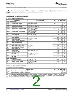
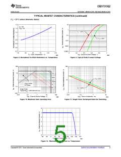
ELECTRICAL CHARACTERISTICS
(TA = 25°C unless otherwise stated)
PARAMETER
Static Characteristics
TEST CONDITIONS
MIN
TYP MAX UNIT
BVDSS
IDSS
Drain to Source Voltage
VGS = 0V, ID = 250mA
30
V
Drain to Source Leakage
Gate to Source Leakage
Gate to Source Threshold Voltage
VGS = 0V, VDS = 24V
VDS = 0V, VGS = +10 / -8V
VDS = VGS, ID = 250mA
VGS = 3V, ID = 4A
1
100
1.8
42
mA
nA
V
IGSS
VGS(th)
0.9
1.3
31
26
24
16
mΩ
mΩ
mΩ
S
RDS(on)
Drain to Source On Resistance
Transconductance
VGS = 4.5V, ID = 4A
VGS = 8V, ID = 4A
32
30
gfs
VDS = 15V, ID = 4A
Dynamic Characteristics
Ciss
Coss
Crss
RG
Input Capacitance
260 340
140 180
pF
pF
pF
Ω
VGS = 0V, VDS = 15V,
f = 1MHz
Output Capacitance
Reverse Transfer Capacitance
Series Gate Resistance
Gate Charge Total (4.5V)
Gate Charge – Gate to Drain
Gate Charge Gate to Source
Gate Charge at Vth
Output Charge
13
1.3
2.1
0.4
0.7
0.3
3.8
2.8
3.9
4.2
1.3
17
2.6
2.7
Qg
nC
nC
nC
nC
nC
ns
ns
ns
ns
Qgd
Qgs
Qg(th)
Qoss
td(on)
tr
VDS = 15V,
ID = 4A
VDS = 13.5V, VGS = 0V
Turn On Delay Time
Rise Time
VDS = 15V, VGS = 4.5V,
ID = 4A, RG = 2Ω
td(off)
tf
Turn Off Delay Time
Fall Time
Diode Characteristics
VSD
Qrr
trr
Diode Forward Voltage
ISD = 4A, VGS = 0V
0.85
6.4
1
V
Reverse Recovery Charge
Reverse Recovery Time
nC
ns
VDD= 13.5V, IF = 4A,
di/dt = 300A/ms
12.9
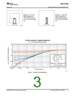
THERMAL CHARACTERISTICS
(TA = 25°C unless otherwise stated)
PARAMETER
MIN
TYP MAX UNIT
7.4 °C/W
RqJC
RqJA
Thermal Resistance Junction to Case(1)
Thermal Resistance Junction to Ambient(1)(2)
67 °C/W
(1)
R
qJC is determined with the device mounted on a 1-inch2 (6.45-cm2), 2-oz. (0.071-mm thick) Cu pad on a 1.5-inch × 1.5-inch (3.81-cm ×
3.81-cm), 0.06-inch (1.52-mm) thick FR4 PCB. RqJC is specified by design, whereas RqJA is determined by the user’s board design.
(2) Device mounted on FR4 material with 1-inch2 (6.45-cm2), 2-oz. (0.071-mm thick) Cu.
2
Submit Documentation Feedback
Copyright © 2010, Texas Instruments Incorporated

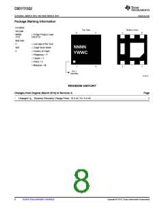
 TI [ TEXAS INSTRUMENTS ]