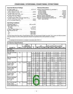
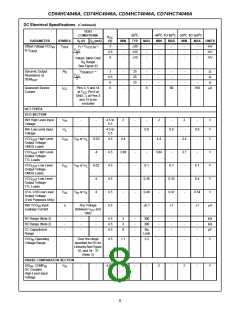
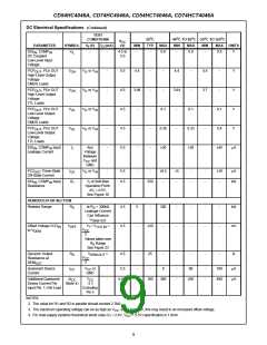
CD54HC4046A, CD74HC4046A, CD54HCT4046A, CD74HCT4046A
frequency. At this stable point the voltage on C2 remains
constant as the PC2 output is in three-state and the VCO
input at pin 9 is a high impedance. Also in this condition,
V
CC
the signal at the phase comparator pulse output (PCP
)
OUT
V
is a HIGH level and so can be used for indicating a locked
DEMOUT (AV)
condition.
Thus, for PC2, no phase difference exists between SIG
IN
1/2 V
CC
and COMP over the full frequency range of the VCO.
IN
Moreover, the power dissipation due to the low-pass filter is
reduced because both p- and n-type drivers are “OFF” for
most of the signal input cycle. It should be noted that the
PLL lock range for this type of phase comparator is equal to
the capture range and is independent of the low-pass filter.
0
o
o
o
With no signal present at SIG , the VCO adjusts, via PC2,
φDEMOUT
0
180
360
IN
to its lowest frequency.
FIGURE 6. PHASE COMPARATOR 3: AVERAGE OUTPUT
VOLTAGE vs INPUT PHASE DIFFERENCE:
Phase Comparator 3 (PC3)
V
= V
DEMOUT
PC3OUT
This is
a positive edge-triggered sequential phase
= (V /2π) (φSIG - φCOMP );
CC IN IN
detector using an RS-type flip-flop. When the PLL is using
this comparator, the loop is controlled by positive signal
φ
= (φSIG - φCOMP )
DEMOUT IN IN
transitions and the duty factors of SIG and COMP are
IN IN
not important. The transfer characteristic of PC3,
assuming ripple (f = f ) is suppressed, is:
r
i
SIG
V
V
= V
=
(V /2p) (fSIG
CC
-
fCOMP )
IN
where
IN
DEMOUT
DEMOUT
PC3OUT
IN
is the demodulator output at pin 10; V
(via low-pass filter).
DEMOUT
COMP
IN
VCO
OUT
The average output from PC3, fed to the VCO via the low-
pass filter and seen at the demodulator at pin 10
PC3
OUT
(V
), is the resultant of the phase differences of
DEMOUT
SIG and COMP
as shown in Figure 6. Typical
V
IN
IN
CC
VCO
IN
waveforms for the PC3 loop locked at f are shown in
o
GND
Figure 7.
FIGURE 7. TYPICAL WAVEFORMS FOR PLL USING PHASE
The phase-to-output response characteristic of PC3
(Figure 6) differs from that of PC2 in that the phase angle
COMPARATOR 3, LOOP LOCKED AT f
o
o
o
between SIG and COMP varies between 0 and 360
IN IN
o
and is 180 at the center frequency. Also PC3 gives a
greater voltage swing than PC2 for input phase differences
but as aconsequence the ripple content of the VCO input
signal is higher. With no signal present at SIG , the VCO
IN
adjusts, via PC3, to its highest frequency.
The only difference between the HC and HCT versions is the
input level specification of the INH input. This input disables
the VCO section. The comparator’s sections are identical, so
that there is no difference in the SIG (pin 14) or COMP
IN
IN
(pin 3) inputs between the HC and the HCT versions.
5

 TI [ TEXAS INSTRUMENTS ]