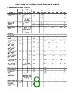
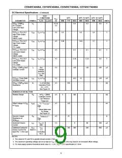
CD54HC4046A, CD74HC4046A, CD54HCT4046A, CD74HCT4046A
C1
6
7
4
3
14
SIG
COMP
C1
C1
B
IN
IN
A
PC1
PC3
OUT
OUT
2
V
REF
R2
R1
S
12
11
D
D
15
Q
Q
-
VCO
R2
R1
R
-
+
V
CC
UP
Q
Q
D
p
10
CP
R
R3
C2
13
DEM
PC2
OUT
D
OUT
-
R5
+
n
Q
Q
V
CC
D
GND
DOWN
CP
R
1
D
PCP
OUT
INH
5
VCO
9
IN
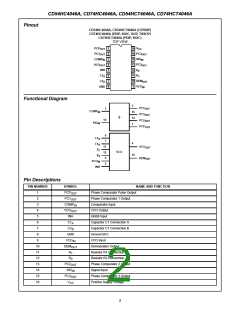
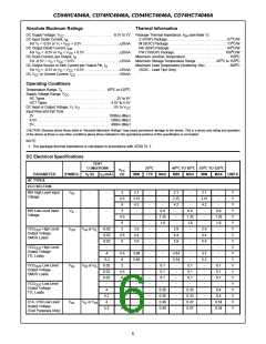
FIGURE 1. LOGIC DIAGRAM
General Description
VCO
Phase Comparators
The signal input (SIG ) can be directly coupled to the self-
IN
The VCO requires one external capacitor C1 (between C1
A
biasing amplifier at pin 14, provided that the signal swing is
between the standard HC family input logic levels.
Capacitive coupling is required for signals with smaller
swings.
and C1 ) and one external resistor R1 (between R and
B
1
GND) or two external resistors R1 and R2 (between R and
1
GND, and R and GND). Resistor R1 and capacitor C1
2
determine the frequency range of the VCO. Resistor R2
enables the VCO to have a frequency offset if required. See
logic diagram, Figure 1.
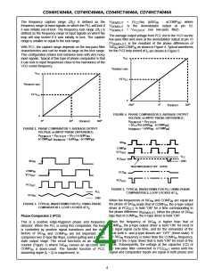
Phase Comparator 1 (PC1)
This is an Exclusive-OR network. The signal and comparator
The high input impedance of the VCO simplifies the design
of low-pass filters by giving the designer a wide choice of
resistor/capacitor ranges. In order not to load the low-pass
filter, a demodulator output of the VCO input voltage is
input frequencies (f ) must have a 50% duty factor to obtain
the maximum locking range. The transfer characteristic of
i
PC1, assuming ripple (f = 2f ) is suppressed, is:
r
i
V
= (V /π) (φSIG - φCOMP ) where V
DEMOUT
CC
IN
IN
DEMOUT
= V
provided at pin 10 (DEM
). In contrast to conventional
OUT
techniques where the DEM
is the demodulator output at pin 10; V
(via low-pass filter).
DEMOUT
PC1OUT
voltage is one threshold
OUT
voltage lower than the VCO input voltage, here the DEM
OUT
voltage equals that of the VCO input. If DEM
is used, a The average output voltage from PC1, fed to the VCO input
OUT
load resistor (R ) should be connected from DEM
to via the low-pass filter and seen at the demodulator output at
S
OUT
should be left open. The VCO pin 10 (V
GND; if unused, DEM
), is the resultant of the phase differences
OUT
DEMOUT
output (VCO
)
can be connected directly to the of signals (SIG ) and the comparator input (COMP ) as
OUT
IN
IN
comparator input (COMP ), or connected via a frequency- shown in Figure 2. The average of V
is equal to 1/2
IN
divider. The VCO output signal has a specified duty factor of
50%. A LOW level at the inhibit input (INH) enables the VCO input the VCO oscillates at the center frequency (f ).
DEM
V
when there is no signal or noise at SIG , and with this
CC
IN
o
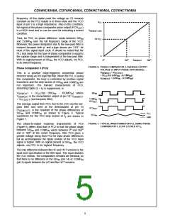
and demodulator, while a HIGH level turns both off to Typical waveforms for the PC1 loop locked at f are shown
o
minimize standby power consumption.
in Figure 3.
3

 TI [ TEXAS INSTRUMENTS ]