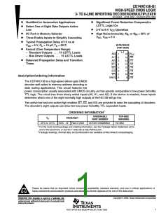
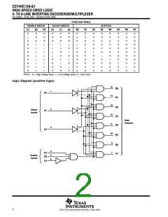
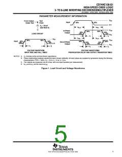
CD74HC138-Q1
HIGH-SPEED CMOS LOGIC
3- TO 8-LINE INVERTING DECODER/DEMULTIPLEXER
SCLS580A − APRIL 2004 − REVISED APRIL 2008
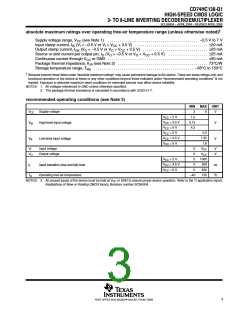
absolute maximum ratings over operating free-air temperature range (unless otherwise noted)†
Supply voltage range, V (see Note 1) . . . . . . . . . . . . . . . . . . . . . . . . . . . . . . . . . . . . . . . . . . . . . . −0.5 V to 7 V
CC
Input clamp current, I (V < −0.5 V or V > V + 0.5 V) . . . . . . . . . . . . . . . . . . . . . . . . . . . . . . . . . . . . . 20 mA
IK
I
I
CC
Output clamp current, I (V < −0.5 V or V > V + 0.5 V) . . . . . . . . . . . . . . . . . . . . . . . . . . . . . . . . . 20 mA
OK
O
O
CC
Source or sink current per output pin, I (V > −0.5 V or V < V + 0.5 V) . . . . . . . . . . . . . . . . . . . . 25 mA
O
O
O
CC
Continuous current through V or GND . . . . . . . . . . . . . . . . . . . . . . . . . . . . . . . . . . . . . . . . . . . . . . . . . . . 50 mA
CC
Package thermal impedance, θ (see Note 2) . . . . . . . . . . . . . . . . . . . . . . . . . . . . . . . . . . . . . . . . . . . . . . 73°C/W
JA
Storage temperature range, T
. . . . . . . . . . . . . . . . . . . . . . . . . . . . . . . . . . . . . . . . . . . . . . . . . . . −65°C to 150°C
stg
†
Stresses beyond those listed under “absolute maximum ratings” may cause permanent damage to the device. These are stress ratings only, and
functional operation of the device at these or any other conditions beyond those indicated under “recommended operating conditions” is not
implied. Exposure to absolute-maximum-rated conditions for extended periods may affect device reliability.
NOTES: 1. All voltages referenced to GND unless otherwise specified.
2. The package thermal impedance is calculated in accordance with JESD 51-7.
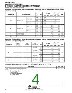
recommended operating conditions (see Note 3)
MIN
2
MAX
UNIT
V
Supply voltage
6
V
CC
IH
V
CC
V
CC
V
CC
V
CC
V
CC
V
CC
= 2 V
1.5
3.15
4.2
= 4.5 V
= 6 V
V
High-level input voltage
V
V
= 2 V
0.5
1.35
1.8
= 4.5 V
= 6 V
V
IL
Low-level input voltage
V
V
Input voltage
0
0
V
CC
V
CC
V
V
I
Output voltage
O
V
CC
V
CC
V
CC
= 2 V
0
1000
500
400
125
= 4.5 V
= 6 V
0
t
Input transition (rise and fall) time
Operating free-air temperature
ns
t
0
T
−40
°C
A
NOTES: 3. All unused inputs of the device must be held at V or GND to ensure proper device operation. Refer to the TI application report,
CC
Implications of Slow or Floating CMOS Inputs, literature number SCBA004.
3
POST OFFICE BOX 655303 • DALLAS, TEXAS 75265

 TI [ TEXAS INSTRUMENTS ]