CC2510Fx / CC2511Fx
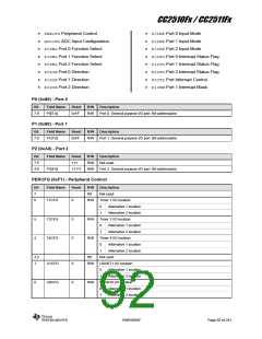
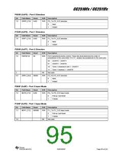
P0DIR (0xFD) - Port 0 Direction
Bit
Field Name
Reset
R/W
Description
7:0
DIRP0_[7:0]
0x00
R/W
P0_7 to P0_0 I/O direction
0
1
Input
Output
P1DIR (0xFE) - Port 1 Direction
Bit
Field Name
Reset
R/W
Description
7:0
DIRP1_[7:0]
0x00
R/W
P1_7 to P1_0 I/O direction
0
1
Input
Output
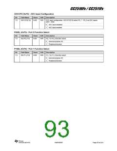
P2DIR (0xFF) - Port 2 Direction
Bit
Field Name
Reset
R/W
Description
7:6
PRIP0[1:0]
00
R/W
Port 0 peripheral priority control. These bits shall determine the order of
precedence in the case when PERCFG assigns two peripherals to the same pins
00
01
10
11
USART0 - USART1
USART1 - USART0
Timer 1 channels 0 and 1 - USART1
Timer 1 channel 2 - USART0
5
-
R0
Not used
4:0
DIRP2_[4:0]
00000
R/W
P2_4 to P2_0 I/O direction
0
1
Input
Output
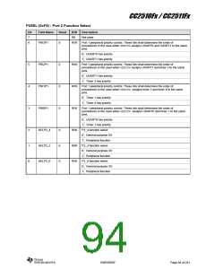
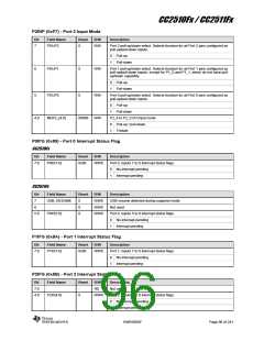
P0INP (0x8F) - Port 0 Input Mode
Bit
Field Name
Reset
R/W
Description
7:0
MDP0_[7:0]
0x00
R/W
P0_7 to P0_0 I/O input mode
0
1
Pull-up / pull-down
Tristate
P1INP (0xF6) - Port 1 Input Mode
Bit
Field Name
Reset
R/W
Description
7:2
MDP1_[7:2]
000000
R/W
P1_7 to P1_2 I/O input mode
0
1
Pull-up / pull-down
Tristate
1:0
-
R0
Not used
SWRS055F
Page 95 of 241

 TI [ TEXAS INSTRUMENTS ]