CC2510Fx / CC2511Fx
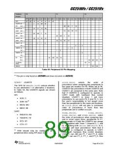
12.4.6.5 Timer 4
The settings in the ADCCFG register override
the settings in P0SEL (the register used to
select a pin to be either GPIO or to have a
peripheral function).
PERCFG.T4CFG selects whether to use
alternative 1 or alternative 2 locations.
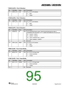
In Table 50, the Timer 4 signals are shown as
follows:
The ADC can be configured to use the
general-purpose I/O pin P2_0 as an external
trigger to start conversions. P2_0 must be
configured as a general-purpose I/O in input
mode, when being used for ADC external
trigger.
• Channel 0 compare pin: 0
• Channel 1 compare pin: 1
P2SEL.PRI3P1,
P2SEL.PRI2P1,
P2SEL.PRI1P1, and P2SEL.PRI0P1 select
the order of precedence when assigning two,
and in some cases three, peripherals to P1.
Setting P2SEL.PRI12P1=1 gives Timer 4
precedence over Timer 1. It is the user’s
responsibility to avoid configurations where the
order of precedence is not conclusive.
Refer to Section 12.10 on Page 137 for a
detailed description on how to use the ADC.
12.4.6.8 Debug Interface
Ports P2_1 and P2_2 are used for debug data
and clock signals, respectively. These are
shown as DD (debug data) and DC (debug
clock) in Table 50. The state of P2SEL is
overridden by the debug interface. Also,
P2DIR.DIRP2_1 and P2DIR.DIRP2_2 is
overridden when the chip changes the
direction to supply the external host with data.
12.4.6.6 I2S
The
I2S
configuration
register
bit
I2SCFG1.IOLOC selects whether to use
alternative 1 or alternative 2 locations.
In Table 50, the I2S signals are shown as
follows:
12.4.6.9 32.768 kHz XOSC Input
• Continuous Serial Clock (SCK): CK
• Word Select: WS
Ports P2_3 and P2_4 are used to connect to
an external 32.768 kHz crystal. These port
pins will be set in analog mode and used by
the 32.768 kHz crystal oscillator when
CLKCON.OSC32K is low, regardless of the
configurations of these pins.
• Serial Data In: RX
• Serial Data Out: TX
If
the
I2S
interface
is
enabled
(I2SCFG0_ENAB=1), the I2S interface will
have precedence in cases where other
peripherals (except for the debug interface)
are configured to be on the same location.
This is the case even if the pins are configured
to be general purpose I/O pins.
12.4.6.10 Radio Test Output Signals
For debug and test purposes, a number of
internal status signals in the radio may be
output on the port pins P1_7 – P1_5. This
debug option is controlled through the RF
registers IOCFG2 - IOCFG0 (see Section 15
for more details).
12.4.6.7 ADC
Setting IOCFGx.GDOx_CFG to a value other
than 0 will override the P1SEL_SELP1_7,
When using the ADC in an application, some
or all of the P0 pins must be configured as
ADC inputs. The port pins are mapped to the
ADC inputs so that P0_7 – P0_0 corresponds
to AIN7 - AIN0. To configure a P0 pin to be
used as an ADC input the corresponding bit in
the ADCCFG register must be set to 1. The
default values in this register select the Port 0
P1SEL_SELP1_6,
and
P1SEL_SELP1_5
settings, and the pins will automatically
become outputs. These pins cannot be used
when the I2S interface is enabled.
12.4.7 I/O Registers
pins
as
non-ADC
input
i.e.
digital
The registers for the IO ports are described in
this section. The registers are:
input/outputs.
Note: P0_6 and P0_7 do not exist on
CC2511Fx, hence six input channels are
available (AIN0 - AIN5)
•
•
•
P0Port 0
P1Port 1
P2Port 2
SWRS055F
Page 91 of 241

 TI [ TEXAS INSTRUMENTS ]