CC2510Fx / CC2511Fx
12.4.3 Low I/O Supply Voltage
•
•
P1IEN: P1 interrupt enables
In applications where the digital I/O power
supply voltage VDD on pin DVDD is below
2.6 V, the register bit IOCFG1.GDO_DSshould
be set to 1.
PICTL: P0/P2 interrupt enables and P0,
P1, and P2 edge configuration
•
•
•
P0IFG: P0 interrupt status flags
P1IFG: P1 interrupt status flags
P2IFG: P2 interrupt status flags
12.4.4 General Purpose I/O Interrupts
General purpose I/O pins configured as inputs
can be used to generate interrupts. The
interrupts can be configured to trigger on
either a rising or falling edge of the external
signal. Each of the P0, P1 and P2 ports have
separate interrupt enable bits common for all
bits within the port located in the IENx
registers as follows:
Note: All port interrupts are blocked when
SLEEP.MODE≠00
12.4.5 General Purpose I/O DMA
When used as general purpose I/O pins, the
P0_1 and P1_3 pins are each associated with
one DMA trigger. These DMA triggers are
IOC_0 for P0_1 and IOC_1 for P1_3 as shown
in Table 51 on Page 104.
•
•
•
IEN1.P0IE: P0 interrupt enable
IEN2.P1IE: P1 interrupt enable
IEN2.P2IE: P2 interrupt enable
The IOC_0 DMA trigger is activated when
there
is
a
rising
edge
on
P0_1
In addition to these common interrupt enables,
the bits within each port have interrupt enable
bits located in I/O port SFRs. Each bit within
P1 has an individual interrupt enable bit,
P1_xIEN, where x is 0 - 7, located in the
P1IEN register. For P0, the low-order nibble
and the high-order nibble have their individual
interrupt enables, P0IENL and P0IENH
respectively, found in the PICTL register. For
the P2_0 – P2_4 inputs there is a common
interrupt enable, P2IEN, in the PICTL
register.
(P0SEL.SELP0_1 and P0DIR.P0_1 must be
0) and IOC_1 is activated when there is a
falling edge on P1_3 (P1SEL.SELP1_3 and
P1DIR.P1_3 must be 0). Note that only input
transitions on pins configured as general
purpose I/O, inputs will produce a DMA trigger.
12.4.6 Peripheral I/O
This section describes how the digital
input/output pins are configured as peripheral
I/Os. For each peripheral unit that can
interface with an external system through the
digital input/output pins, a description of how
peripheral I/Os are configured is given in the
following sub-sections.
When an interrupt condition occurs on one of
the
general
purpose
I/O
pins,
the
corresponding interrupt status flag in the P0 -
P2 interrupt status flag registers, P0IFG ,
P1IFG, or P2IFG will be set to 1. The
interrupt status flag is set regardless of
whether the pin has its interrupt enable set.
The CPU interrupt flags located in IRCON2for
P1 and P2, and IRCON for P0, will only be
asserted if one or more of the interrupt enable
bits found in P1IEN (P1) and PICTL (P0 and
P2) are set to 1. Note that the module interrupt
flag needs to be cleared prior to clearing the
CPU interrupt flag.
In general, setting the appropriate PxSEL bits
to 1 is required to select peripheral I/O function
on a digital I/O pin.
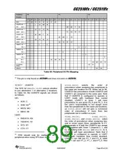
Note that peripheral units have two alternative
locations for their I/O pins. Please see Table
50.
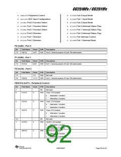
The SFRs used for I/O interrupts are
described in Section 1.1 on Page 57. The
registers are the following:
SWRS055F
Page 88 of 241

 TI [ TEXAS INSTRUMENTS ]