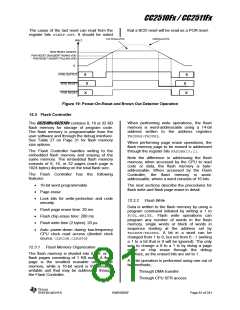
CC2510Fx / CC2511Fx
write operation is initiated, program execution
will resume from the next instruction when the
Flash Controller has completed the operation.
The flash erase operation requires that the
instruction that starts the erase i.e. writing to
FCTL.ERASE is followed by a NOP instruction
as shown in the example code. Omitting the
NOP instruction after the flash erase operation
will lead to undefined behavior.
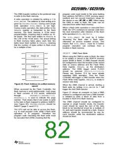
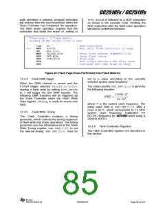
; Erase page 1 in flash memory
; Assumes 26 MHz system clock is used
;
CLR
MOV
JB
MOV
MOV
MOV
NOP
RET
EA
A,FCTL
ACC.7,C1
FADDRH,#02h
FWT,#2Ah
FCTL,#01h
; Mask interrupts
; Wait until flash controller is ready
C1:
; Setup flash address (FADDRH[5:1]=1)
; Setup flash timing
; Erase page
; Must always execute a NOP after erase
; Continues here when flash is ready
Figure 25: Flash Page Erase Performed from Flash Memory
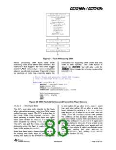
12.3.4 Flash DMA trigger
set to a value according to the currently
selected system clock frequency.
When the DMA channel is armed and the
FLASH trigger selected TRIG[4:0]=10010,
starting a flash write by setting FCTL.WRITE
to 1 will trigger the first DMA transfer. The
following DMA transfers will be triggered by
the Flash Controller when the Flash Write
Data register, FWDATA, is ready to receive new
data.
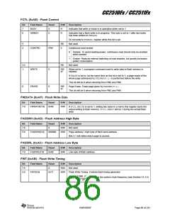
The value used for FWT.FWT[5:0]is given by
the following equation:
21000⋅ F
FWT =
16⋅109
where F is the system clock frequency. The
initial value held in FWT.FWT[5:0] after a
reset is 0x11, which corresponds to 13 MHz
system clock frequency (calibrated HS
RCOSC frequency for CC2510Fx when using a
26 MHz XOSC).
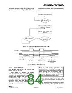
12.3.5 Flash Write Timing
The Flash Controller contains
a
timing
generator, which controls the timing sequence
of flash write and erase operations. The timing
generator uses the information set in the Flash
Write Timing register, FWT.FWT[5:0], to set
the internal timing. FWT.FWT[5:0] must be
12.3.6 Flash Controller Registers
The Flash Controller registers are described in
this section.
SWRS055F
Page 85 of 241

 TI [ TEXAS INSTRUMENTS ]