CC2510Fx / CC2511Fx
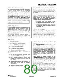
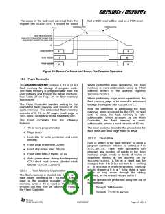
The cause of the last reset can read from the
that a BOD reset will be read as a POR reset.
register bits SLEEP.RST. It should be noted
1.8V REGULATED
UNREGULATED
VOLT
BOD RESET ASSERT
POR RESET DEASSERT RISING VDD
POR RESET ASSERT FALLING VDD
0
POR OUTPUT
X
X
X
BOD RESET
POR RESET
X
X
X
Figure 19: Power-On-Reset and Brown Out Detector Operation
12.3 Flash Controller
When performing write operations, the flash
memory is word-addressable using a 14-bit
address written to the address registers
FADDRH:FADDRL.
The CC2510Fx/CC2511Fx contains 8, 16 or 32 KB
flash memory for storage of program code.
The flash memory is programmable from the
user software and through the debug interface.
See Table 27 on Page 31 for flash memory
size options.
When performing page erase operations, the
flash memory page to be erased is addressed
through the register bits FADDRH[5:1].
The Flash Controller handles writing to the
embedded flash memory and erasing of the
same memory. The embedded flash memory
consists of 8, 16, or 32 pages (each page is
1024 bytes) depending on the total flash size.
Note the difference in addressing the flash
memory; when accessed by the CPU to read
code or data, the flash memory is byte-
addressable. When accessed by the Flash
Controller, the flash memory is word-
addressable, where a word consists of 16 bits.
The Flash Controller has the following
features:
• 16-bit word programmable
• Page erase
The next sections describe the procedures for
flash write and flash page erase in detail.
• Lock bits for write-protection and code
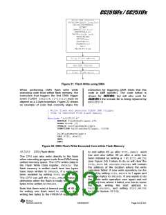
12.3.2 Flash Write
security
Data is written to the flash memory by using a
program command initiated by writing a 1 to
FCTL.WRITE. Flash write operations can
program any number of words in the flash
memory, single words or block of words in
sequence starting at the address set by
FADDRH:FADDRL. A bit in a word can be
changed from 1 to 0, but not from 0 - 1 (writing
a 1 to a bit that is 0 will be ignored). The only
way to change a 0 to a 1 is by doing a page
erase or chip erase through the debug
interface, as the erased bits are set to 1.
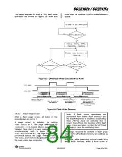
• Flash page erase time: 20 ms
• Flash chip erase time: 200 ms
• Flash write time (2 bytes): 20 µs
• Auto power-down during low-frequency
CPU clock read access (divided clock
source, CLKCON.CLKSPD)
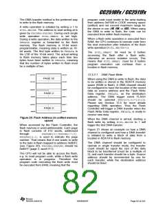
12.3.1 Flash Memory Organization
The flash memory is divided into 8, 16, or 32
flash pages consisting of 1 KB each. A flash
page is the smallest erasable unit in the
memory, while a 16-bit word is the smallest
writable unit that may be addressed through
the Flash Controller.
A write operation is performed using one out of
two methods;
• Through DMA transfer
• Through CPU SFR access
SWRS055F
Page 81 of 241

 TI [ TEXAS INSTRUMENTS ]