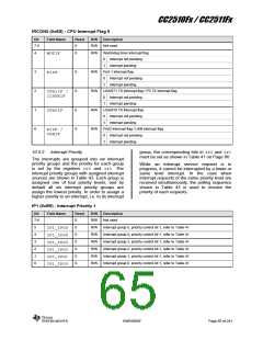
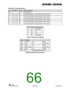
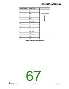
CC2510Fx / CC2511Fx
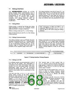
Note that after the Debug Lock bit has
changed due to a Flash Information Page write
or a flash mass erase, a HALT, RESUME,
The lock protect bits are written as a normal
flash write to FWDATA(see Section 12.3.2), but
the Debug Interface needs to select the Flash
Information Page first instead of the Flash
Main Page which is the default setting. The
Information Page is selected through the
Debug Configuration which is written through
the Debug Interface only. Refer to Section
11.4.1 and Table 46 for details on how the
Flash Information Page is selected using the
Debug Interface.
DEBUG_INSTR,
STEP_INSTR,
or
STEP_REPLACE command must be executed
so that the Debug Lock value returned by
READ_STATUS shows the updated Debug
Lock value. For example a dummy NOP
DEBUG_INSTR command could be executed.
The Debug Lock bit will also be updated after
a device reset so an alternative is to reset the
chip and reenter debug mode.
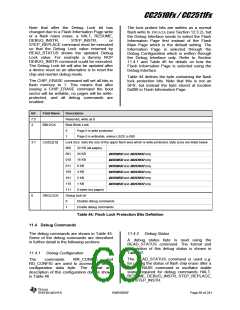
Table 44 defines the byte containing the flash
lock protection bits. Note that this is not an
SFR, but instead the byte stored at location
0x000 in Flash Information Page.
The CHIP_ERASE command will set all bits in
flash memory to 1. This means that after
issuing a CHIP_ERASE command the boot
sector will be writable, no pages will be write-
protected, and all debug commands are
enabled.
Bit
7:5
4
Field Name
Description
Reserved, write as 0
Boot Block Lock
BBLOCK
0
1
Page 0 is write protected
Page 0 is writeable, unless LSIZE is 000
3:1
LSIZE[2:0]
Lock Size. Sets the size of the upper flash area which is write-protected. Byte sizes are listed below
000
001
010
011
100
101
110
111
32 KB (all pages)
24 KB
CC2510F32 and CC2511F32 only
CC2510F32 and CC2511F32 only
CC2510F32 and CC2511F32 only
CC2510F32 and CC2511F32 only
CC2510F32 and CC2511F32 only
CC2510F32 and CC2511F32 only
16 KB
8 KB
4 KB
2 KB
1 KB
0 bytes (no pages)
0
DBGLOCK
Debug lock bit
0
1
Disable debug commands
Enable debug commands
Table 44: Flash Lock Protection Bits Definition
11.4 Debug Commands
The debug commands are shown in Table 45.
Some of the debug commands are described
in further detail in the following sections
11.4.2 Debug Status
A debug status byte is read using the
READ_STATUS command. The format and
description of this debug status is shown in
Table 47.
11.4.1 Debug Configuration
The READ_STATUS command is used e.g.
for polling the status of flash chip erase after a
CHIP_ERASE command or oscillator stable
status required for debug commands HALT,
RESUME, DEBUG_INSTR, STEP_REPLACE,
and STEP_INSTR.
The
commands
WR_CONFIG
and
RD_CONFIG are used to access the debug
configuration data byte. The format and
description of this configuration data is shown
in Table 46
SWRS055F
Page 69 of 241

 TI [ TEXAS INSTRUMENTS ]