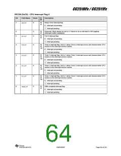
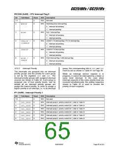
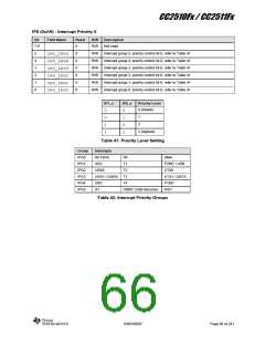
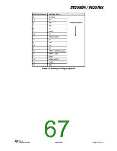
CC2510Fx / CC2511Fx
11 Debug Interface
The debug interface uses the I/O pins P2_1 as
Debug Data and P2_2 as Debug Clock during
Debug mode. These I/O pins can be used as
general purpose I/O only while the device is
not in Debug mode. Thus the debug interface
does not interfere with any peripheral I/O pins.
The CC2510Fx/CC2511Fx includes an on-chip
debug module which communicates over a
two-wire interface. The debug interface allows
programming of the on-chip flash. It also
provides access to memory and registers
contents, and debug features such as
breakpoints, single-stepping, and register
modification.
11.1 Debug Mode
Debug mode is entered by forcing two rising
edge transitions on pin P2_2 (Debug Clock)
while the RESET_N input is held low.
Note: Debugging of PM2 and PM3 is not
supported. Also note that CLKCON.CLKSPD
must be 000 or 001 when using the debug
interface
While in Debug mode pin P2_1 is the Debug
Data bi-directional pin and P2_2 is the Debug
Clock input pin.
11.2 Debug Communication
The debug interface uses an SPI-like two-wire
interface consisting of the P2_1 (Debug Data)
and P2_2 (Debug Clock) pins. Data is driven
on the bi-directional Debug Data pin at the
positive edge of Debug Clock and data is
sampled on the negative edge of this clock.
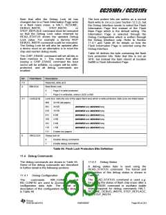
Debug commands are sent by an external host
and consist of 1 to 4 output bytes (including
command byte) from the host and an optional
input byte read by the host. Command and
data is transferred with MSB first. Figure 17
shows a timing diagram of data on the debug
interface.
Figure 17: Debug Interface Timing Diagram
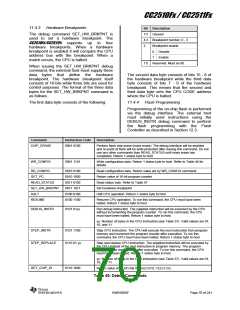
11.3 Debug Lock Bit
For software and/or access protection, a set of
lock bits can be written. This information is
contained in the Flash Information Page (see
Section 10.2.3.2), at location 0x000. The Flash
Information Page can only be accessed
through the debug interface. There are three
kinds of lock protect bits as described in this
section.
The second type of lock protect bits is
BBLOCK, which is used to lock the boot sector
page (page 0 ranging from address 0x0000 to
0x03FF). When BBLOCK is set to 0, the boot
sector page is locked.
The third type of lock protect bit is DBGLOCK,
which is used to disable hardware debug
support through the Debug Interface. When
DBGLOCK is set to 0, almost all debug
commands are disabled.
The lock size bits LSIZE[2:0] are used to
define which section of the flash memory
should be write protected, if any. The size of
the write protected area can be set to 0 (no
pages), 1, 2, 4, 8, 16, 24, or 32 KB (all pages),
starting from top of flash memory and defining
a section below this. Note that for CC2510F8,
CC2511F8, CC2510F16, and CC2511F16, the only
supported value for LSIZE[2:0]is 0 and 7
(all or no pages respectively).
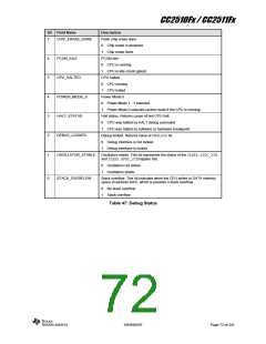
When the Debug Lock bit, DBGLOCK, is set to
0 (see Table 44) all debug commands except
CHIP_ERASE,
READ_STATUS
and
GET_CHIP_ID are disabled and will not
function. The status of the Debug Lock bit can
be read using the READ_STATUS command
(see Section 11.4.2).
SWRS055F
Page 68 of 241

 TI [ TEXAS INSTRUMENTS ]