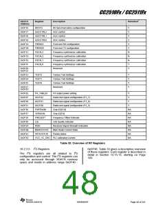
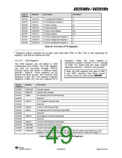
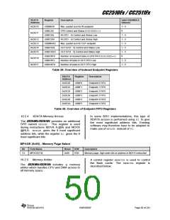
CC2510Fx / CC2511Fx
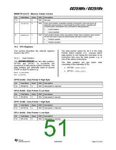
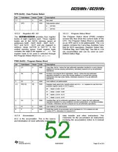
DPS (0x92) - Data Pointer Select
Bit
7:1
0
Field Name
Reset
R/W
R/W
R/W
Description
Not used
0
0
DPS
Data pointer select
0
1
DPTR0
DPTR1
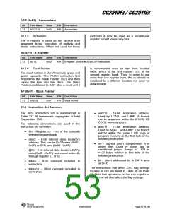
10.3.2 Registers R0 - R7
10.3.3 Program Status Word
The Program Status Word (PSW) contains
several bits that show the current state of the
CPU. The Program Status Word is accessible
as an SFR and it is bit-addressable. The PSW
register contains the Carry flag, Auxiliary Carry
flag for BCD operations, Register Select bits,
Overflow flag, and Parity flag. Two bits in PSW
are uncommitted and can be used as user-
defined status flags.
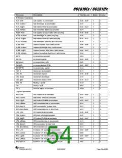
The CC2510Fx/CC2511Fx provides four register
banks of eight registers each. These register
banks are in the DATA memory space at
addresses 0x00 - 0x07, 0x08 - 0x0F, 0x10 -
0x17 and 0x18 - 0x1F and are mapped to
address range 0xFF00 to 0xFF1F in the
unified memory space. Each register bank
contains the eight 8-bit register R0 - R7. The
register bank to be used is selected through
the Program Status Word PSW.RS[1:0].
PSW (0xD0) - Program Status Word
Bit
Field Name
Reset
R/W
Description
7
CY
0
R/W
Carry flag. Set to 1 when the last arithmetic operation resulted in a carry (during
addition) or borrow (during subtraction), otherwise cleared to 0 by all arithmetic
operations.
6
AC
0
R/W
Auxiliary carry flag for BCD operations. Set to 1 when the last arithmetic
operation resulted in a carry into (during addition) or borrow from (during
subtraction) the high order nibble, otherwise cleared to 0 by all arithmetic
operations.
5
F0
0
R/W
R/W
User-defined, bit-addressable
4:3
RS[1:0]
00
Register bank select bits. Selects which set of R7- R0registers to use from four
possible register banks in DATA space.
00
01
10
11
Bank 0, 0x00 - 0x07
Bank 1, 0x08 - 0x0F
Bank 2, 0x10 - 0x17
Bank 3, 0x18 - 0x1F
2
OV
0
R/W
Overflow flag, set by arithmetic operations. Set to 1 when the last arithmetic
operation resulted in a carry (addition), borrow (subtraction), or overflow (multiply
or divide). Otherwise, the bit is cleared to 0 by all arithmetic operations.
1
0
F1
P
0
0
R/W
R/W
User-defined, bit-addressable
Parity flag, parity of accumulator set by hardware to 1 if it contains an odd
number of 1’s, otherwise it is cleared to 0
10.3.4 Accumulator
data transfer and other instructions. The
mnemonic for the accumulator (in instructions
involving the accumulator) refers to A instead
of ACC.
ACC is the accumulator. This is the source
and destination of most arithmetic instructions,
SWRS055F
Page 52 of 241

 TI [ TEXAS INSTRUMENTS ]