CC2510Fx / CC2511Fx
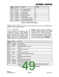
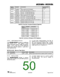
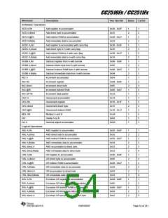
XDATA
Address
Register
Description
Valid USBINDEX
Value(s)
0xDE10
USBMAXI
USBCS0
Max. packet size for IN endpoint
1 - 5
0
EP0 Control and Status (USBINDEX=0)
IN EP{1 - 5} Control and Status Low
IN EP{1 - 5} Control and Status High
Max. packet size for OUT endpoint
OUT EP{1 - 5} Control and Status Low
OUT EP{1 - 5} Control and Status High
Number of received bytes in EP0 FIFO (USBINDEX=0)
Number of bytes in OUT FIFO Low
Number of bytes in OUT FIFO High
0xDE11
USBCSIL
USBCSIH
USBMAXO
USBCSOL
USBCSOH
USBCNT0
USBCNTL
USBCNTH
1 - 5
1 - 5
1 - 5
1 - 5
1 - 5
0xDE12
0xDE13
0xDE14
0xDE15
0
0xDE16
0xDE17
1 - 5
1 - 5
Table 35: Overview of Indexed Endpoint Registers
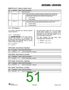
XDATA
Register
Description
Address
0xDE20
0xDE22
0xDE24
0xDE26
0xDE28
0xDE2A
USBF0
USBF1
USBF2
USBF3
USBF4
USBF5
Endpoint 0 FIFO
Endpoint 1 FIFO
Endpoint 2 FIFO
Endpoint 3 FIFO
Endpoint 4 FIFO
Endpoint 5 FIFO
Table 36: Overview of Endpoint FIFO Registers
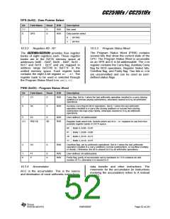
10.2.4 XDATA Memory Access
In some 8051 implementations, this type of
XDATA access is performed using P2 to give
the most significant address bits. Existing
software may therefore have to be adapted to
make use of MPAGE instead of P2.
The CC2510Fx/CC2511Fx provides an additional
SFR named MPAGE. This register is used
during instructions MOVX A,@Ri and MOVX
@Ri,A. MPAGE gives the 8 most significant
address bits, while the register Ri gives the 8
least significant bits.
MPAGE (0x93) - Memory Page Select
Bit
Field Name
Reset
R/W
Description
7:0
MPAGE[7:0]
0x00
R/W
Memory page, high-order bits of address in MOVX instruction
10.2.5 Memory Arbiter
A control register MEMCTR is used to control
the flash cache. The MEMCTR register is
described below.
The CC2510Fx/CC2511Fx includes a memory
arbiter which handles CPU and DMA access to
all memory space.
SWRS055F
Page 50 of 241

 TI [ TEXAS INSTRUMENTS ]