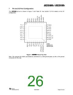
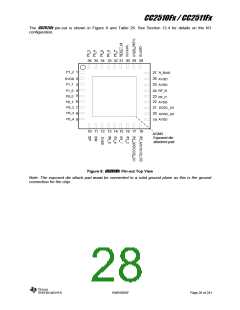
CC2510Fx / CC2511Fx
6.15 Timer Inputs AC Characteristics
TA = 25°C, VDD = 3.0 V if nothing else stated. All measurement results are obtained using the
CC2510EM reference designs ([1]).
Parameter
Min
Typ
Max
Unit Condition/Note
Synchronizers determine the shortest input pulse
Input capture pulse width
tSYSCLK
that can be recognized. The synchronizers operate
from the current system clock rate (see Table 19)
Table 23: Timer Inputs AC Characteristics
6.16 DC Characteristics
The DC Characteristics of CC2510Fx/CC2511Fx are listed in Table 24 below.
TA = 25°C, VDD = 3.0 V if nothing else stated. All measurement results are obtained using the
CC2510EM reference designs ([1]).
Digital Inputs/Outputs
Min
Typ
Max
Unit Condition
Logic "0" input voltage
30
%
%
Of VDD supply (2.0 - 3.6 V)
Logic "1" input voltage
70
NA
NA
Of VDD supply (2.0 - 3.6 V)
Input equals 0 V
Logic "0" input current per pin
Logic "1" input current per pin
Total logic “0” input current all pins
Total logic “1” input current all pins
I/O pin pull-up and pull-down resistor
12
12
70
70
nA
nA
nA
nA
kΩ
Input equals VDD
20
Table 24: DC Characteristics
SWRS055F
Page 25 of 241

 TI [ TEXAS INSTRUMENTS ]