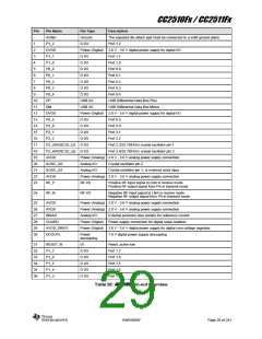
CC2510Fx / CC2511Fx
Pin
-
Pin Name
AGND
P1_2
DVDD
P1_1
P1_0
P0_0
P0_1
P0_2
P0_3
P0_4
DP
Pin Type
Ground
D I/O
Description
The exposed die attach pad must be connected to a solid ground plane
Port 1.2
1
2
Power (Digital) 2.0 V - 3.6 V digital power supply for digital I/O
3
D I/O
Port 1.1
4
D I/O
Port 1.0
5
D I/O
Port 0.0
6
D I/O
Port 0.1
7
D I/O
Port 0.2
8
D I/O
Port 0.3
9
D I/O
Port 0.4
10
11
12
13
14
15
16
17
18
19
20
21
22
23
USB I/O
USB I/O
USB Differential Data Bus Plus
USB Differential Data Bus Minus
DM
DVDD
P0_5
P2_0
P2_1
P2_2
Power (Digital) 2.0 V - 3.6 V digital power supply for digital I/O
D I/O
D I/O
D I/O
D I/O
Port 0.5
Port 2.0
Port 2.1
Port 2.2
P2_3/XOSC32_Q1 D I/O
P2_4/XOSC32_Q2 D I/O
Port 2.3/32.768 kHz crystal oscillator pin 1
Port 2.4/32.768 kHz crystal oscillator pin 2
AVDD
Power (Analog) 2.0 V - 3.6 V analog power supply connection
XOSC_Q2
XOSC_Q1
AVDD
Analog I/O
Analog I/O
Crystal oscillator pin 2
Crystal oscillator pin 1, or external clock input
Power (Analog) 2.0 V - 3.6 V analog power supply connection
RF_P
RF I/O
Positive RF input signal to LNA in receive mode
Positive RF output signal from PA in transmit mode
24
RF_N
RF I/O
Negative RF input signal to LNA in receive mode
Negative RF output signal from PA in transmit mode
25
26
27
28
29
30
AVDD
Power (Analog) 2.0 V - 3.6 V analog power supply connection
Power (Analog) 2.0 V - 3.6 V analog power supply connection
AVDD
RBIAS
Analog I/O
External precision bias resistor for reference current
GUARD
AVDD_DREG
DCOUPL
Power (Digital) Power supply connection for digital noise isolation
Power (Digital) 2.0 V - 3.6 V digital power supply for digital core voltage regulator
Power
1.8 V digital power supply decoupling
decoupling
31
32
33
34
35
36
RESET_N
P1_7
DI
Reset, active low
Port 1.7
D I/O
D I/O
D I/O
D I/O
D I/O
P1_6
Port 1.6
P1_5
Port 1.5
P1_4
Port 1.4
P1_3
Port 1.3
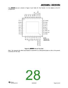
Table 26: CC2511Fx Pin-out Overview
SWRS055F
Page 29 of 241

 TI [ TEXAS INSTRUMENTS ]