CC2510Fx / CC2511Fx
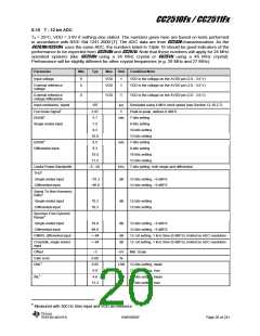
6.10 7 - 12 bit ADC
TA = 25°C, VDD = 3.0V if nothing else stated. The numbers given here are based on tests performed
in accordance with IEEE Std 1241-2000 [7]. The ADC data are from CC2430 characterization. As the
CC2510x/C2511Fx uses the same ADC, the numbers listed in Table 18 should be good indicators of the
performance to be expected from CC2510x and CC2511x. Note that these numbers will apply for 24 MHz
operated systems (like CC2510x using a 24 MHz crystal or CC2511x using a 48 MHz crystal).
Performance will be slightly different for other crystal frequencies (e.g. 26 MHz and 27 MHz).
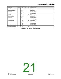
Parameter
Min
Typ
Max
Unit Condition/Note
Input voltage
0
0
VDD
VDD
V
V
VDD is the voltage on the AVDD pin (2.0 - 3.6 V)
External reference
voltage
VDD is the voltage on the AVDD pin (2.0 - 3.6 V)
External reference
voltage differential
0
VDD
V
VDD is the voltage on the AVDD pin (2.0 - 3.6 V)
Input resistance, signal
Full-Scale Signal5
ENOB5
197
2.97
5.7
Simulated using 4 MHz clock speed (see Section 12.10.2.7)
kΩ
V
Peak-to-peak, defines 0 dBFS
7-bits setting
bits
Single ended input
7.5
9-bits setting
9.3
10-bits setting
10.8
6.5
12-bits setting
ENOB5
bits
7-bits setting
Differential input
8.3
9-bits setting
10.0
11.5
0 - 20
10-bits setting
12-bits setting
Useful Power Bandwidth
THD5
kHz
dB
7-bits setting, both single and differential
-Single ended input
-Differential input
−75.2
−86.6
12-bits setting, −6 dBFS
12-bits setting, −6 dBFS
Signal To Non-Harmonic
Ratio5
-Single ended input
-Differential input
70.2
79.3
dB
12-bits setting
12-bits setting
Spurious Free Dynamic
Range5
-Single ended input
-Differential input
78.8
88.9
dB
12-bits setting, −6 dBFS
12-bits setting, −6 dBFS
CMRR, differential input
<−84
<−84
dB
dB
12- bit setting, 1 kHz Sine (0 dBFS), limited by ADC resolution
12- bit setting, 1 kHz Sine (0 dBFS), limited by ADC resolution
Crosstalk, single ended
input
Offset
−3
0.68
0.05
0.9
mV
%
Mid. Scale
Gain error
DNL5
LSB
12-bits setting, mean
12-bits setting, max
12-bits setting, mean
12-bits setting, max
INL5
4.6
LSB
13.3
5 Measured with 300 Hz Sine input and VDD as reference
SWRS055F
Page 20 of 241

 TI [ TEXAS INSTRUMENTS ]